


11 11
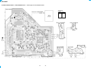
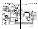
4-1. IC PIN DESCRIPTION
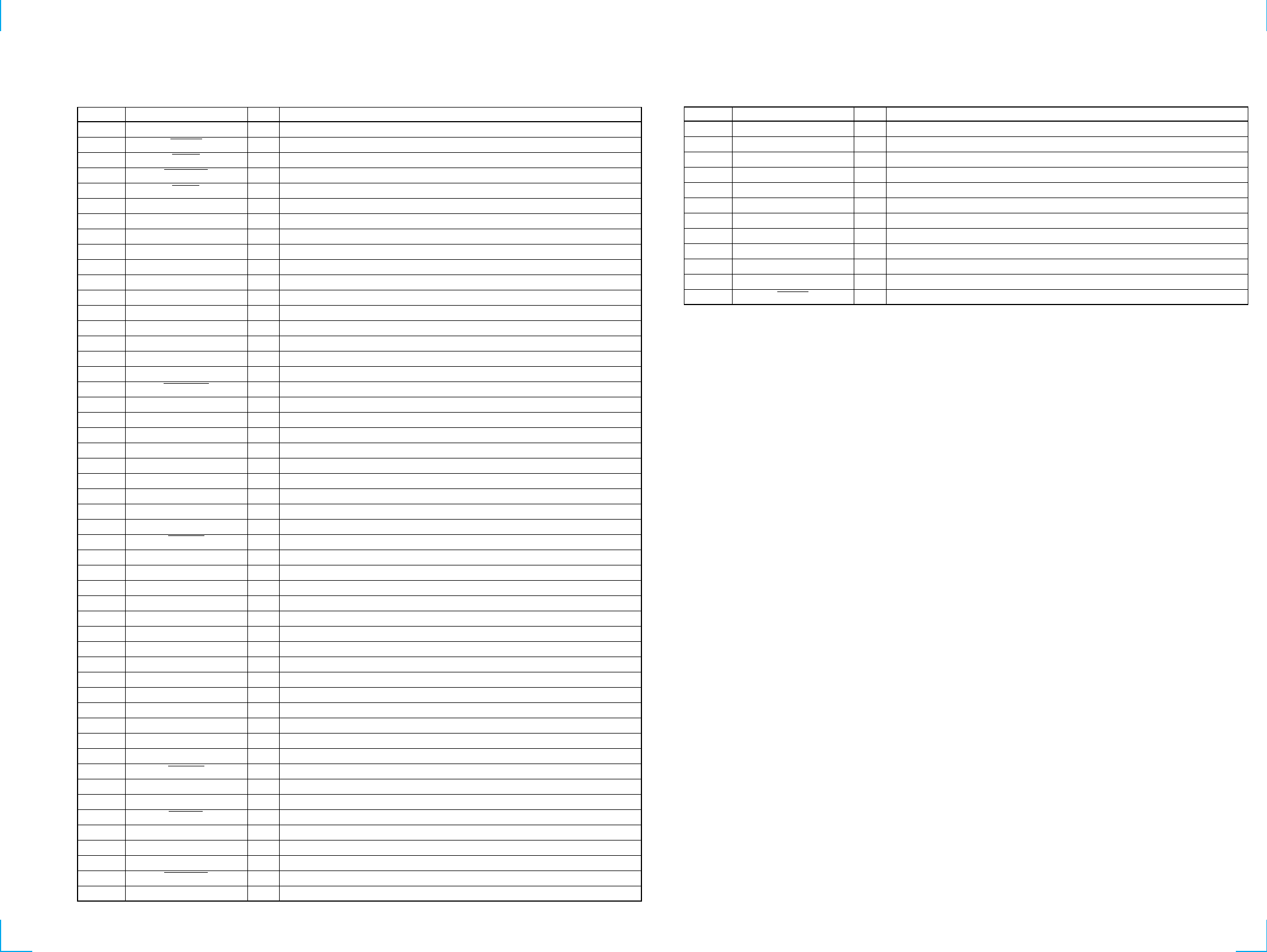
• IC801 µPD17705GC-547-3B9 (SYSTEM CONTROL)
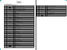
Pin No. Pin Name I/O Pin Description
1 NC — Not used. (Connect to ground in this set.)
2 IN_SW I Disc insertion detection input L: IN_SW
3 D_SW I DOWN switch detection input L: D_SW
4 SELF_SW I Disc self store detection input L: SELF_SW
5 L_SW I Sled limit switch detection input L: L_SW
6 LM_EJ O Loading motor control output (Eject direction)
7 LM_LD O Loading motor control output (Loading direction)
8 RY_ON O Relay control output
9, 10 NC — Not used. (Open)
11 BAND_SW I BAND select input 0: US
12 – 20 NC — Not used. (Open)
21 GND3 — Ground
22 NC — Not used. (Open)
23 ADKI2 I A/D key input 2
24 ADKI1 I A/D key input 1
25 ROTCOM I Rotary commander shift key input
26 NC — Not used. (Open)
27 TEST_SW I Test mode initial setting detection input L: TEST_SW
28, 29 NC — Not used. (Open)
30 VDD2 — Power supply pin (+5 V)
31 FMIN I PLL local oscillator frequency input
32 NC — Not used. (Open)
33 GND2 — Ground
34 NC — Not used. (Open)
35 EO1 O PLL error 1 output
36 TEST0 — Connect to GND line.
37 – 40 NC — Not used. (Open)
41 ACC_IN I Accessory power detection input L: ACC_IN
42 SCOR I SCOR signal detection input
43 MUTE O Mute control output
44 LEVEL D O Level control output
45 NC — Not used. (Open)
46 PH2 I Connect to +5 V line.
47 LEVEL 1 O Volume control output
48, 49 NC O Not used. (Open)
50 EMPH_O O Emphasis control output
51 PW_ON O System power control output
52 LM_ON O Loading motor power control output
53 CD_ON O CD power control output
54 ILLON O Illumination power control output
55 – 57 NC — Not used. (Open)
58 LCD_CE O LCD chip enable output
59 EZ_SEL I Rotary commander shift key input L: EZ_SEL
60 SENS I CD SENS signal detection input
61 FOK I Focus OK signal detection input
62 LD_ON O Laser ON/OFF control output L: LD_ON
63, 64 NC — Not used. (Open)
65 LCD_CLK O LCD serial clock output
66 LCD_DAT O LCD serial data output
67 LCD_INH O LCD inhibition output L: LCD_INH
68 SQCK0 O Sub Q read clock output
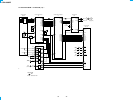
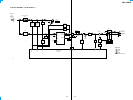
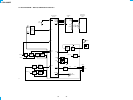
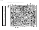
SECTION 4
DIAGRAMS
Pin No. Pin Name I/O Pin Description
69 CD_RST O Reset output to CD signal processor IC.
70 SQ_SI I Sub Q data input
71 CD_SO0 O CD signal serial data output
72 CD_LAT O CD signal processing data latch output
73 CD_CK0 O CD signal processing serial clock output
74 NC — Not used. (Open)
75 GND1 — Ground
76 XOUT O ceramic oscillator output (4.5 MHz)
77 XIN I ceramic oscillator input (4.5 MHz)
78 BU_IN I Backup power detection input
79 VDD1 — Power supply pin (+5 V)
80 RESET I Reset input L: RESET