


1997 Jun 12 6
Philips Semiconductors Product specification
2 W BTL audio amplifier TDA8543
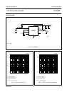
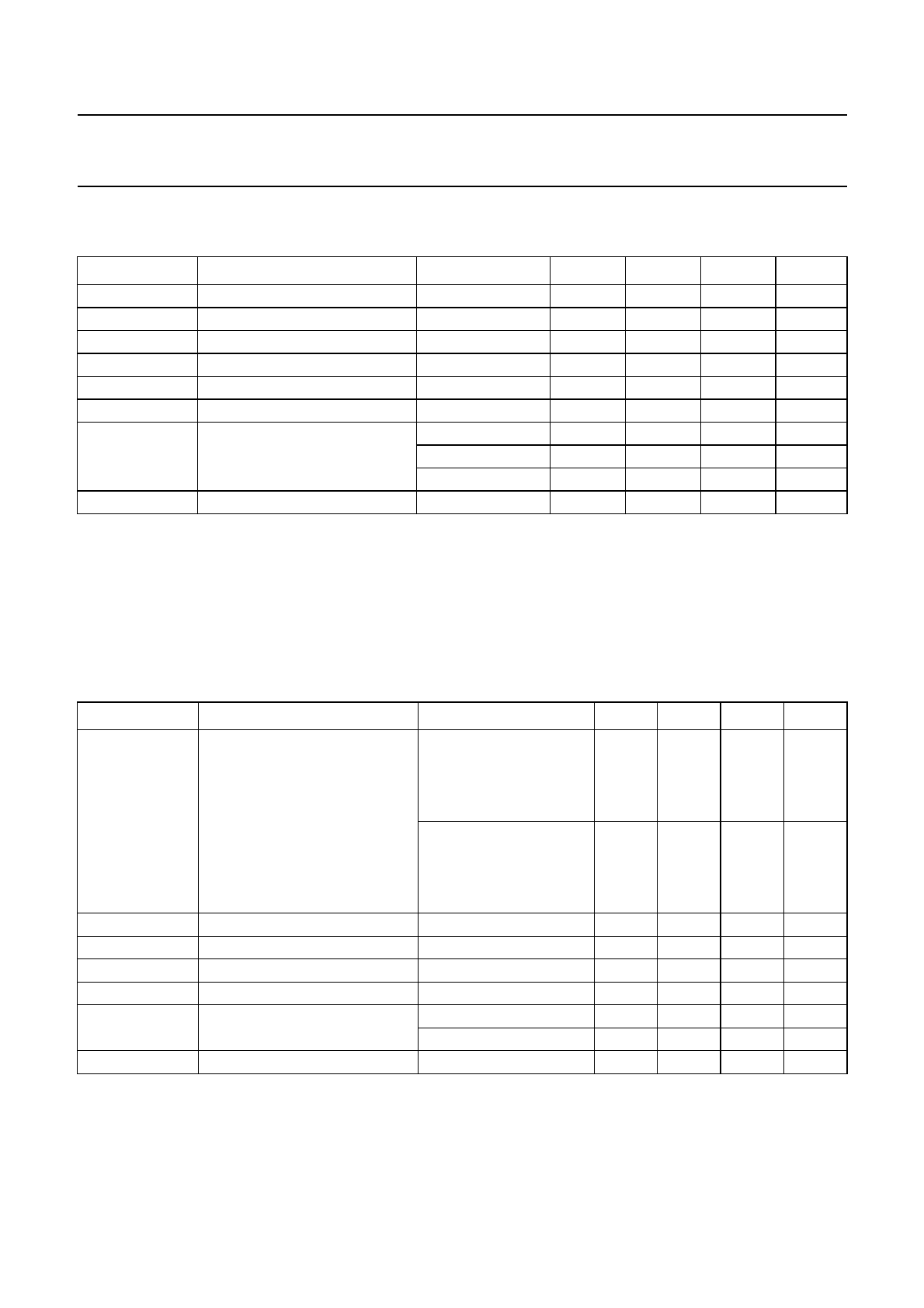
DC CHARACTERISTICS
V
CC
=5V; T
amb
=25°C; R
L
=8Ω; V
MODE
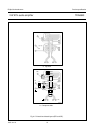
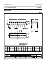
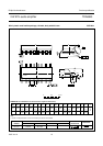
= 0 V; G = 20 dB; measured in test circuit Fig.4; unless otherwise specified.
Notes
1. With a load connected at the outputs the quiescent current will increase, the maximum of this increase being equal
to the DC output offset voltage divided by R
L
.
2. The DC output voltage with respect to ground is approximately 0.5 × V
CC
.
AC CHARACTERISTICS
V
CC
=5V; T
amb
=25°C; R
L
=8Ω; f = 1 kHz; V
MODE
= 0 V; G = 20 dB; measured in test circuit Fig.4; unless otherwise
specified.
SYMBOL PARAMETER CONDITIONS MIN. TYP. MAX. UNIT
V
CC
supply voltage operating 2.2 5 18 V
I
q
quiescent current R
L
= ∞; note 1 − 812mA
I
stb
standby current V
MODE
=V
CC
−−10 µA
V
O
DC output voltage note 2 − 2.2 − V
V
OUT+
− V
OUT−
differential output voltage offset −−50 mV
I
IN+
, I
IN−
input bias current −−500 nA
V
MODE
input voltage mode select operating 0 − 0.5 V
mute 1.5 − V
CC
− 1.5 V
standby V
CC
− 0.5 − V
CC
V
I
MODE
input current mode select 0 < V
MODE
<V
CC
−−20 µA
SYMBOL PARAMETER CONDITIONS MIN. TYP. MAX. UNIT
P
o
output power THD = 10%;
V
CC
= 5 V; R
L
=8Ω 1 1.2 − W
V
CC
= 7.5 V; R
L
=8Ω− 2.2 − W
V
CC
= 9 V; R
L
=16Ω− 2.0 − W
THD = 0.5%;
V
CC
= 5 V; R
L
=8Ω 0.6 0.9 − W
V
CC
= 7.5 V; R
L
=8Ω− 1.7 − W
V
CC
= 9 V; R
L
=16Ω− 1.4 − W
THD total harmonic distortion P
o
= 0.5 W − 0.15 0.3 %
G
v
closed loop voltage gain note 1 6 − 30 dB
Z
i
differential input impedance − 100 − kΩ
V
no
noise output voltage note 2 −−100 µV
SVRR supply voltage ripple rejection note 3 50 −−dB
note 4 40 −−dB
V
o
output voltage in mute condition note 5 −−200 µV