


1997 Jun 12 3
Philips Semiconductors Product specification
2 W BTL audio amplifier TDA8543
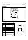
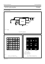
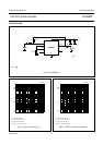
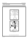
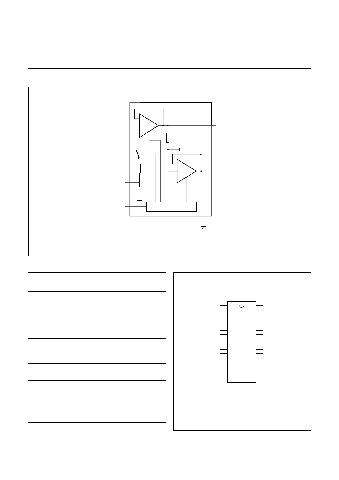
BLOCK DIAGRAM
Fig.1 Block diagram.
handbook, halfpage
MGK402
6
STANDBY/MUTE LOGIC
5
12
4
3
13
14
11
R
R
20 kΩ
20 kΩ
IN−
IN+
V
CC
SVR
MODE
OUT−
OUT+
GND
−
−
+
−
−
+
TDA8543
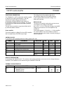
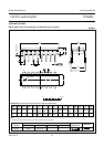
PINNING
SYMBOL PIN DESCRIPTION
n.c. 1 not connected
n.c. 2 not connected
MODE 3 operating mode select
(standby, mute, operating)
SVR 4 half supply voltage, decoupling
ripple rejection
IN+ 5 positive input
IN− 6 negative input
n.c. 7 not connected
n.c. 8 not connected
n.c. 9 not connected
n.c. 10 not connected
OUT− 11 negative loudspeaker terminal
V
CC
12 supply voltage
GND 13 ground
OUT+ 14 positive loudspeaker terminal
n.c. 15 not connected
n.c. 16 not connected
Fig.2 Pin configuration.
handbook, halfpage
TDA8543
MGK401
1
2
3
4
5
6
7
8
16
15
14
13
12
11
10
9
n.c.
n.c.
MODE
SVR
IN+
IN−
n.c.
n.c.
n.c
n.c.
OUT−
V
CC
GND
OUT+
n.c
n.c.