


1998 Apr 01 6
Philips Semiconductors Product specification
2 × 1 W BTL audio amplifier TDA8542
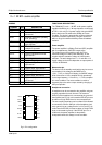
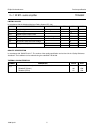
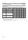
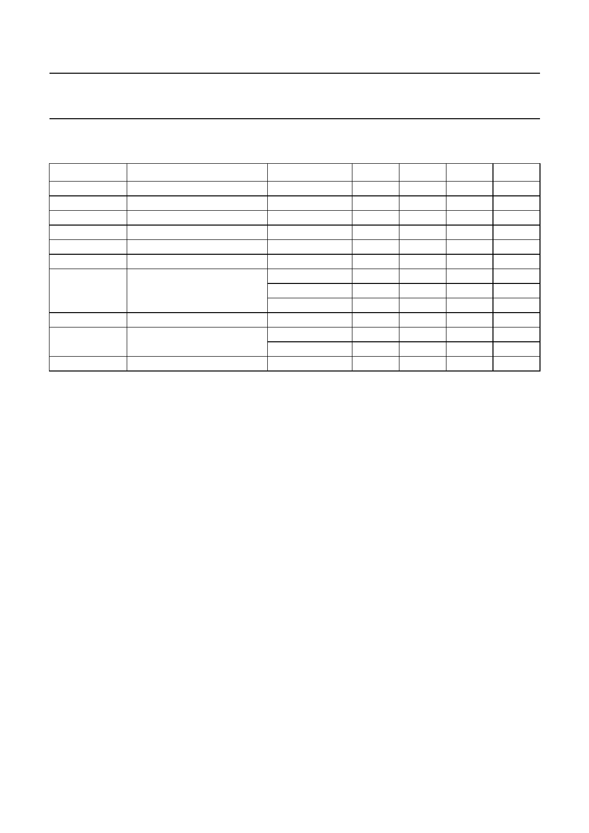
DC CHARACTERISTICS
V
CC
=5V; T
amb
=25°C; R
L
=8Ω; V
MODE
= 0 V; measured in test circuit Fig.3; unless otherwise specified.
Notes
1. With a load connected at the outputs the quiescent current will increase, the maximum of this increase being equal
to the DC output offset voltage divided by R
L
.
2. The DC output voltage with respect to ground is approximately 0.5 × V
CC
.
SYMBOL PARAMETER CONDITIONS MIN. TYP. MAX. UNIT
V
CC
supply voltage operating 2.2 5 18 V
I
q
quiescent current R
L
= ∞; note 1 − 15 22 mA
I
stb
standby current V
MODE
=V
CC
−−10 µA
V
O
DC output voltage note 2 − 2.2 − V
V
OUT+
− V
OUT−
differential output voltage offset −−50 mV
I
IN+
, I
IN−
input bias current −−500 nA
V
MODE
input voltage mode select operating 0 − 0.5 V
mute 1.5 − V
CC
− 1.5 V
standby V
CC
− 0.5 − V
CC
V
I
MODE
input current mode select 0 < V
MODE
<V
CC
−−20 µA
V
BS
input voltage BTL/SE pin single-ended 0 − 0.6 V
BTL 2 − V
CC
V
I
BS
input current BTL/SE pin V
BS
=0 −−100 µA