


1997 Jul 15 6
Philips Semiconductors Product specification
Stereo BTL audio output amplifier with DC
volume control
TDA7053A
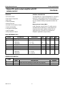
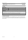
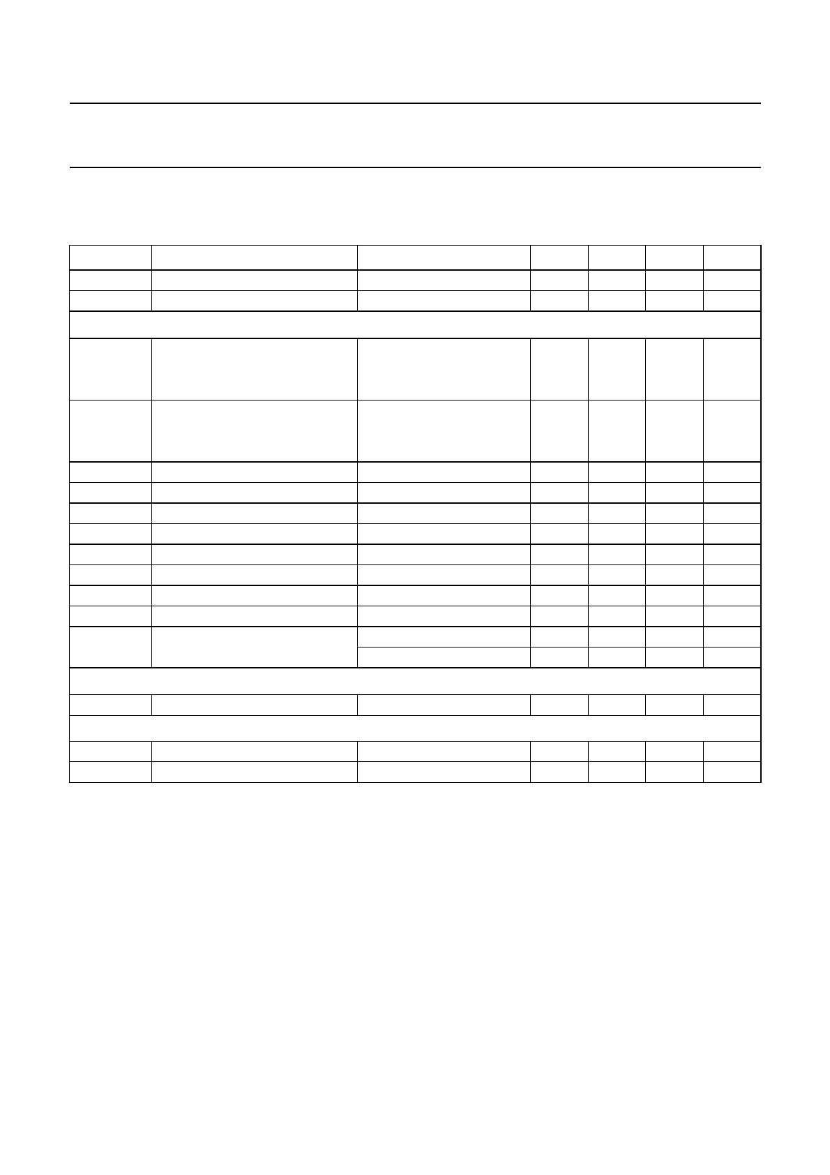
CHARACTERISTICS
V
P
=6V; T
amb
=25°C; f
i
= 1 kHz; TDA7053A: R
L
=8Ω; TDA7053AT: R
L
=16Ω; unless otherwise specified
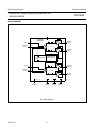
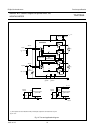
(see Fig.13).
Notes
1. With a load connected to the outputs the quiescent current will increase, the maximum value of this increase being
equal to the DC output offset voltage divided by R
L
.
2. The noise output voltage (RMS value) at f
i
= 500 kHz is measured with R
S
=0Ω and bandwidth = 5 kHz.
3. 20 Hz to 300 kHz (typical).
4. The ripple rejection is measured with R
S
=0Ω and f
i
= 100 Hz to 10 kHz. The ripple voltage of 200 mV (RMS value)
is applied to the positive supply rail.
5. The channel unbalance is measured with V
DC1
=V
DC2
.
6. The channel unbalance at G
1
= 0 dB is measured with V
DC1
=V
DC2
.
7. The noise output voltage (RMS value) is measured with R
S
=5kΩ unweighted.
SYMBOL PARAMETER CONDITIONS MIN. TYP. MAX. UNIT
V
P
supply voltage 4.5 − 18 V
I
q(tot)
total quiescent current V
P
=6V; R
L
=∞; note 1 − 22 25 mA
Maximum gain; V
2,8
≥ 1.4 V
P
out
output power THD = 10%
TDA7053A 1.0 1.1 − W
TDA7053AT 0.5 0.55 − W
THD total harmonic distortion
TDA7053A P
out
= 0.5 W − 0.3 1 %
TDA7053AT P
out
= 0.25 W − 0.3 1 %
G
v
voltage gain 39.5 40.5 41.5 dB
V
I(rms)
input signal handling (RMS value) G
v
= 0 dB; THD < 1% 1 −−V
V
no
noise output voltage f
i
= 500 kHz; note 2 − 210 −µV
B bandwidth at −1dB − note 3 − Hz
SVRR supply voltage ripple rejection note 4 34 38 − dB
V
O(os)
DC output offset voltage V
16
− V
13
and V
12
− V
9
− 0 200 mV
Z
i
input impedance (pins 4 and 6) 15 20 25 kΩ
α
cs
channel separation R
S
=5kΩ 40 −−dB
G
v
channel unbalance note 5 −−1dB
G
1
= 0 dB; note 6 −−1dB
Mute position; V
2,8
= 0.4 V ±30 mV
V
O
output voltage in mute position V
i
= 1.0 V; note 7 − 30 40 µV
DC volume control
G
C
gain control 68.5 73.5 − dB
I
DC
volume control current V
2
=V
8
=0V −20 −25 −30 µA