


1995 Feb 07 7
Philips Semiconductors Preliminary specification
Video output amplifier TDA6111Q
Notes
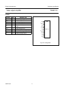
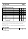
1. If the difference between V
DDL
and V
ip
is less than 7 V, overshoot cannot be specified.
2. SVRR: The ratio of the change in supply voltage to the change in input voltage when there is no change in output
voltage.
O
v
cathode output voltage overshoot V
ocAC
= 100 V (p-p);
V
ocDC
= 100 V square
wave; f < 1 MHz;
t
r
=t
f
=22ns;
see Figs 4 and 5; note 1
− 9 − %
SVRRH high supply voltage rejection ratio f < 50 kHz; note 2 − 85 − dB
SVRRL low supply voltage rejection ratio f < 50 kHz; note 2 − 70 − dB
SYMBOL PARAMETER CONDITIONS MIN. TYP. MAX. UNIT
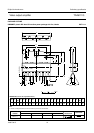
Cathode output
The cathode output is protected against peak currents
(caused by positive voltage peaks during high-resistance
flash) of 5 A maximum with a charge content of 100 µC.
The cathode is also protected against peak currents
(caused by positive voltage peaks during low-resistance
flash) of 10 A maximum with a charge content of 100 nC.
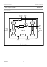
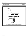
Flashover protection
The TDA6111Q incorporates protection diodes against
CRT flashover discharges that clamp the cathode output
pin to the V
DDH
pin. The DC supply voltage at the V
DDH
pin
has to be within the operating range of 180 to 210 V to
ensure that the Absolute Maximum Rating for V
DDH
of
250 V will not be exceeded during flashover. To limit the
diode current, an external 680 Ω carbon high-voltage
resistor in series with the cathode output and a 2 kV spark
gap are needed (for this resistor-value, the CRT has to be
connected to the main PCB). This addition produces an
increase in the rise and fall times of approximately 5 ns
and a decrease in the overshoot of approximately 4%.
V
DDH
to GND must be decoupled:
1. With a capacitor >20 nF with good HF behaviour
(e.g. foil). This capacitance must be placed as close
as possible to pins 6 and 4, but definitely within 5 mm.
2. With a capacitor >10 µF on the picture tube base print
(common for three output stages).
V
DDL
to GND must be decoupled:
1. With a capacitor >20 nF with good HF behaviour
(e.g. ceramic). This capacitance must be placed as
close as possible to pins 2 and 4, but definitely within
10 mm.
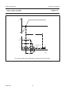
Switch-off behaviour
The switch-off behaviour of the TDA6111Q is defined:
when the bias current becomes zero, at V
DDL
(pin 2) lower
than approximately 5 V, all the output pins
(pins 7, 8 and 9) will be high.