


9397 750 14728 © Koninklijke Philips Electronics N.V. 2005. All rights reserved.
Product data sheet Rev. 02 — 28 April 2005 7 of 16
Philips Semiconductors
TDA6107AJF
Triple video output amplifier
[1] The ratio of the change in supply voltage to the change in input voltage when there is no change in output voltage.
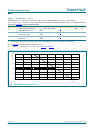
[2] See Figure 6 for the typical DC-to-DC transfer of V
i
to V
oc
.
[3] f < 1 MHz; t
r
=t
f
= 40 ns [pins V
i(1)
,V
i(2)
and V
i(3)
]; see Figure 7 and Figure 8.
t
st
settling time input (50 %) to
output (99 % to 101 %)
V
oc
= 100 V (p-p) square
wave
[3]
- - 350 ns
SR slew rate between
50 V to V
DD
− 50 V
V
i
= 2.5 V (p-p) square
wave
[3]
- 900 - V/µs
O
v
cathode output voltage
overshoot
V
oc
= 100 V (p-p) square
wave
[3]
-2-%
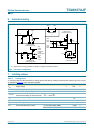
Table 5: Characteristics
…continued
Operating range: T
j
=
−
20
°
C to +150
°
C; V
DD
= 180 V to 210 V; test conditions: T
amb
=25
°
C; V
DD
= 200 V;
V
oc(1)
=V
oc(2)
=V
oc(3)
=
1
⁄
2
V
DD
;C
L
=10pF(C
L
consists of parasitic and cathode capacitance); R
th(h-a)
= 18 K/W; measured in
test circuit of
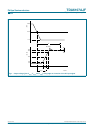
Figure 9; unless otherwise specified.
Symbol Parameter Conditions Min Typ Max Unit
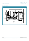
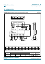
Fig 6. Typical DC-to-DC transfer of V
i
to V
oc
mce455
80
120
40
160
200
V
oc
(V)
0
V
i
(V)
0 4321