


9397 750 14728 © Koninklijke Philips Electronics N.V. 2005. All rights reserved.
Product data sheet Rev. 02 — 28 April 2005 10 of 16
Philips Semiconductors
TDA6107AJF
Triple video output amplifier
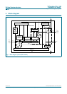
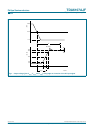
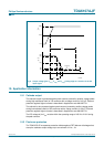
To limit the diode current an external 1.5 kΩ carbon high-voltage resistor in series with the
cathode output and a 2 kV spark gap are needed (for this resistor value, the CRT has to
be connected to the main PCB).
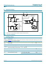
V
DD
must be decoupled to GND:
1. With a capacitor > 20 nF with good HF behavior (e.g. foil); this capacitor must be
placed as close as possible to pins V
DD
and GND and must be within 5 mm.
2. With a capacitor > 3.3 µF on the picture tube base print, depending on the CRT size.
10.3 Switch-off behavior
The switch-off behavior of the TDA6107AJF is controllable. This is because the output
pins of the TDA6107AJF are still under control of the input pins for low power supply
voltages (approximately 30 V and higher).
10.4 Bandwidth
The addition of the flash resistor produces a decreased bandwidth and increases the rise
and fall times.
10.5 Dissipation
A distinction must first be made between static dissipation (independent of frequency) and
dynamic dissipation (proportional to frequency).
The static dissipation of the TDA6107AJF is due to voltage supply currents and load
currents in the feedback network and CRT.
The static dissipation P
stat
equals: P
stat
=V
DD
× I
DD
+3× V
oc
× I
oc
Where:
V
DD
= supply voltage
I
DD
= supply current
V
oc
= DC value of cathode output voltage
I
oc
= DC value of cathode output current
The dynamic dissipation P
dyn
equals: P
dyn
=3× V
DD
× (C
L
+C
int
) × f
i
× V
oc(p-p)
×δ
Where:
C
L
= load capacitance
C
int
= internal load capacitance (≈4 pF)
f
i
= input frequency
V
oc(p-p)
= cathode output voltage (peak-to-peak value)
δ = non-blanking duty cycle
The TDA6107AJF must be mounted on the picture tube base print to minimize the load
capacitance.