


July 1994 6
Philips Semiconductors Product specification
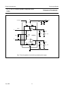
2 x 12 W hi-fi audio power amplifiers with
mute
TDA2616/TDA2616Q
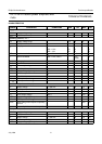
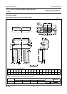
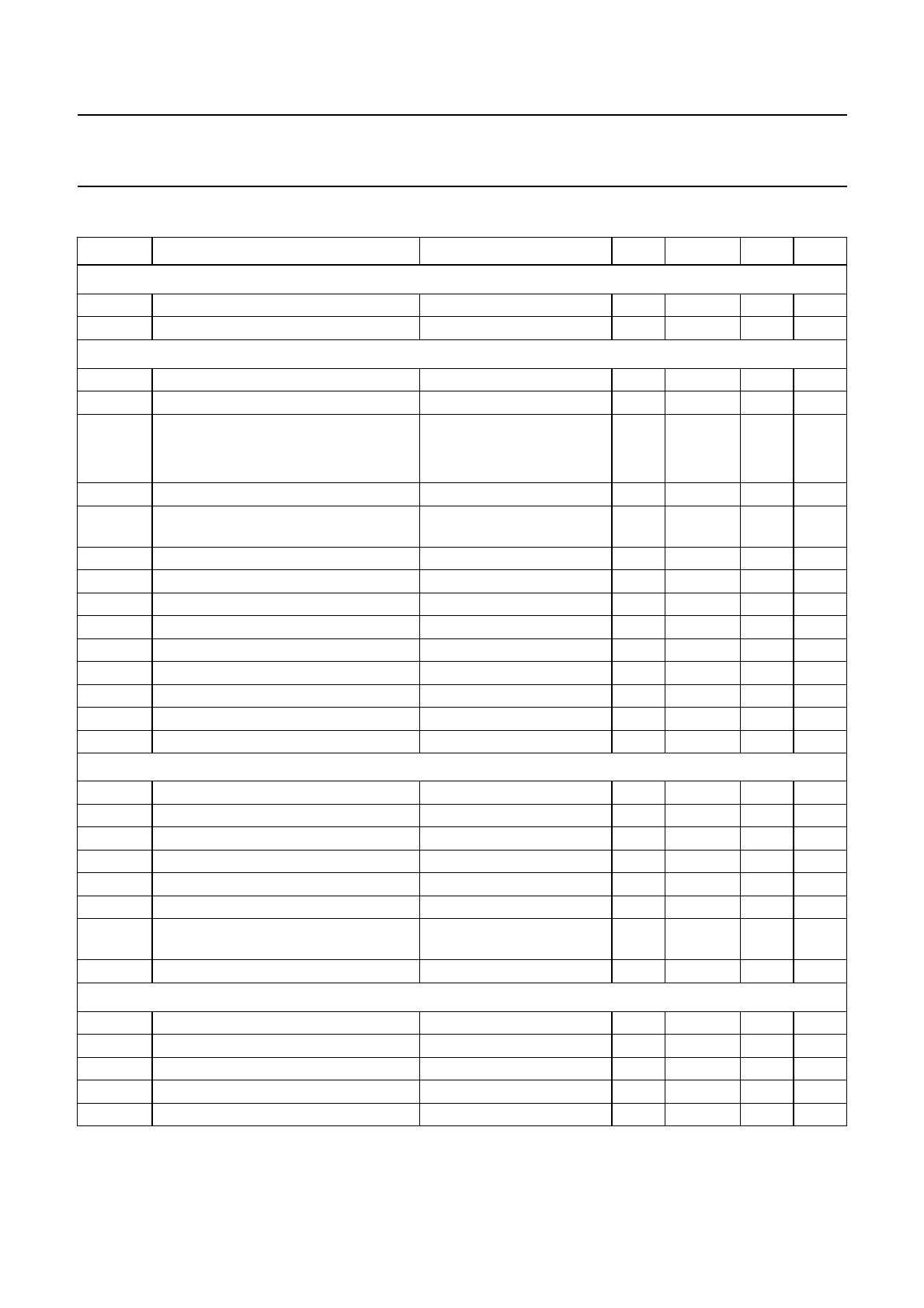
CHARACTERISTICS
SYMBOL PARAMETER CONDITIONS MIN. TYP. MAX. UNIT
Supply
±V
P
supply voltage range − 16 21 V
I
ORM
repetitive peak output current − 2.2 − A
Operating position; note 1
±V
P
supply voltage range 7.5 16 21 V
I
P
total quiescent current R
L
= ∞ 18 40 70 mA
P
O
output power
THD = 0.5% 10 12 − W
THD = 10% 12 15 − W
THD total harmonic distortion P
O
= 6 W − 0.15 0.2 %
B power bandwidth THD = 0.5%; note 2 − 20 to
20 000
− Hz
G
v
voltage gain 29 30 31 dB
G
v
gain unbalance − 0.2 1 dB
V
no
noise output voltage note 3 − 70 140 µV
Z
i
input impedance 14 20 26 kΩ
SVRR supply voltage ripple rejection note 4 40 60 − dB
α channel separation R
S
= 0 46 70 − dB
I
bias
input bias current − 0.3 −µA
∆V
GND
DC output offset voltage − 30 200 mV
∆V
4-6
DC output offset voltage between two channels − 4 150 mV
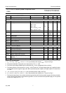
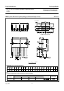
MUTE POSITION (AT I
MUTE
≥ 300 µA)
V
O
output voltage V
I
= 600 mV − 0.3 1.0 mV
Z
2-7
mute input impedance note 7 6.7 9 11.3 kΩ
I
P
total quiescent current R
L
= ∞ 18 40 70 mA
V
no
noise output voltage note 3 − 70 140 µV
SVRR supply voltage ripple rejection note 4 40 55 − dB
∆V
GND
DC output offset voltage − 40 200 mV
∆V
off
offset voltage with respect to operating
position
− 4 150 mV
I
2
current if pin 2 is connected to pin 5 −− 8.2 mA
Mute position; note 5
±V
P
supply voltage range 2 − 5.8 V
I
P
total quiescent current R
L
= ∞ 930 40mA
V
O
output voltage V
I
= 600 mV − 0.3 1.0 mV
V
no
noise output voltage note 3 − 70 140 µV
SVRR supply voltage ripple rejection note 4 40 55 − dB