


2003 Feb 12 13
Philips Semiconductors Preliminary specification
70 W high efficiency power amplifier
with diagnostic facility
TDA1562Q; TDA1562ST;
TDA1562SD
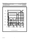
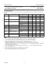
AC CHARACTERISTICS
V
P
= 14.4 V; R
L
=4Ω; R
s
=0Ω; f = 1 kHz; T
amb
=25°C; measurements in accordance with Fig.9; unless otherwise
specified.
Notes
1. The low frequency power roll-off is determined by the value of the electrolytic lift capacitors.
2. The low frequency gain roll-off is determined by the value of the input coupling capacitors.
3. Supply voltage ripple rejection is measured across R
L
; ripple voltage V
ripple(max)
= 2 V (p-p).
4. Common mode rejection ratio is measured across R
L
; common mode voltage V
cm(max)
= 2 V (p-p).
CMMR (dB) = differential gain (G
v
) + common mode attenuation (α
cm
). Test set-up according to Fig.10; mismatch of
input coupling capacitors excluded.
5. Input signal rejection ratio is measured across R
L
; input voltage V
i(max)
= 2 V (p-p). ISSR (dB) = different gain
(G
v
) + mute attenuation (α
m
).
6. Noise output voltage is measured in a bandwidth of 20 Hz to 20 kHz.
7. Noise output voltage is independent of source impedance R
s
.
SYMBOL PARAMETER CONDITIONS MIN. TYP. MAX. UNIT
P
o
output power class-B; THD = 10% 16 19 − W
class-H; THD = 10% 60 70 − W
class-H; THD = 0.5% 45 55 − W
f
ro(h)(P)
high frequency power roll-off P
o
(−1 dB); THD = 0.5%;
note 1
− 20 − kHz
THD total harmonic distortion P
o
=1W − 0.03 − %
P
o
=20W − 0.06 − %
DDD active − 2.1 − %
G
v
voltage gain 25 26 27 dB
f
ro(h)(G)
high frequency gain roll-off G
v
(−1 dB); note 2 20 −−kHz
Z
i(dif)
differential input impedance 90 150 210 kΩ
SVRR supply voltage ripple
rejection
on and mute; note 3 55 63 − dB
standby; note 3 − 90 − dB
CMRR common mode rejection
ratio
on; note 4 56 80 − dB
ISRR input signal rejection ratio mute; note 5 80 100 − dB
V
n(o)
noise output voltage on; note 6 − 100 150 µV
mute; notes 6 and 7 − 60 −µV