


July 1994 7
Philips Semiconductors Product specification
2 x 22 W BTL stereo car radio power
amplifier
TDA1552Q
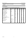
AC CHARACTERISTICS
V
P
= 14.4 V; R
L
= 4 Ω; f = 1 kHz; T
amb
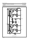
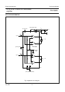
= 25 °C; measurements taken using Fig.3; unless otherwise specified
Notes to the characteristics
1. The circuit is DC adjusted at V
P
= 6 V to 18 V and AC operating at V
P
= 8.5 V to 18 V.
2. At 18 V < V
P
< 30 V the DC output voltage ≤ V
P
/2.
3. Conditions:
a) V
11
= 0 V
b) short-circuit to GND
c) switch V
11
to MUTE or ON condition (rise time ≥ 10 µs).
4. Frequency response externally fixed.
5. Ripple rejection measured at the output with a source impedance of 0 Ω (maximum ripple amplitude of 2 V).
6. Frequency f = 100 Hz.
7. Frequency between 1 kHz and 10 kHz.
8. Noise voltage measured in a bandwidth of 20 Hz to 20 kHz.
9. Noise output voltage independent of R
S
(V
I
= 0 V).
PARAMETER CONDITIONS SYMBOL MIN. TYP. MAX. UNIT
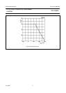
Output power THD = 0.5% P
o
15 17 − W
THD = 10% P
o
20 22 − W
Output power at V
P
= 13.2 V THD = 0.5% P
o
− 12 − W
THD = 10% P
o
− 17 - W
Total harmonic distortion P
o
= 1 W THD − 0.1 − %
Power bandwidth THD = 0.5%
P
o
= −1 dB
w.r.t. 15 W B
w
- 20 to − Hz
15000
Low frequency roll-off note 4
−1 dB f
L
− 25 − Hz
High frequency roll-off −1 dB f
H
20 −−kHz
Closed loop voltage gain G
v
25 26 27 dB
Supply voltage ripple rejection notes 5, 6 RR 42 −−dB
ON notes 5, 7 RR 48 −−dB
mute notes 5, 6, 7 RR 48 −−dB
stand-by notes 5, 6, 7 RR 80 −−dB
Input impedance |Z
i
| 506075kΩ
Noise output voltage
(RMS value)
ON R
S
= 0 Ω; note 8 V
no(rms)
- 70 120 µV
ON R
S
= 10 kΩ; note 8 V
no(rms)
− 100 −µV
mute notes 8, 9 V
no(rms)
− 60 −µA
Channel separation α 40 −−dB
Channel unbalance |∆G
v
|- − 1dB