


Philips Semiconductors Product data
SA58605Dual operational amplifier and 2.5 V shunt regulator
2003 Nov 12
6
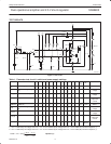
APPLICATION INFORMATION
The SA58605 may be used for various voltage control applications
in which the input threshold voltage exceed 2.5 V for Amp “A” and
154 mV for Amp “B”. When either or both input threshold voltage is
exceeded the output is pulled LOW. The output is connected to V
CC
with a pull-up resistance.
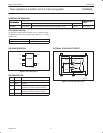
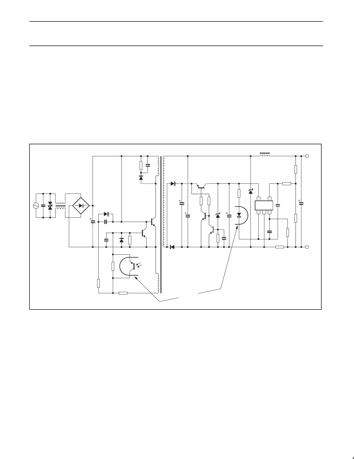
Figure 7 shows the schematic for a Universal Converter/Charger
circuit in which the SA58605 Amp “A” is used to monitor the B+ level
of the converter/charger. Amp “B” input is pulled to ground through a
390 Ω resistor and will remain there. The input to the Amp “A” is
maintained at 0.5 × B+ with the voltage divider of the two 1.5 kΩ
resistors. As B+ drops below 5 V, the input to Amp “A” of the
SA58605 follows and drops below 2.5 V. This causes the output
(pin 1) to go HIGH and the LED is turned off. Q1 base drive is
reduced and Q2 is increased. Thus, the PW modulation is
increased, and B+ is able to satisfy the load requirements of the
battery and circuitry. As B+ is increased above 5 V, it causes the
input to Amp “A” to increase above 2.5 V. Then, the output goes
LOW and the LED is activated which turns on the detection diode.
This increases the drive on Q1 and pulls down the base of Q2
reducing it base drive. With Q2 conducting less, the PW modulation
is decreased and B+ is reduced. Under quasi-steady state, B+ is
maintained at 5 V.
D1
D2
0.033 pF
8.2 kΩ
Q1
8.3 µF
/250 V
L1
10 mH
Q2
2.7 kΩ
100 Ω
V
IN
= 85 – 265 VAC
0.1 µF
100 Ω
MUR160
56 kΩ
0.001 µF
/1 kV
D4
SA58605
5 4
1 32
390 Ω
Q4
Q3
100 µF
/16 V
800 µF
/8 V
1 MΩ
47 kΩ
D3
100Ω
0.1 µF
0.1 µF
0.22 Ω
390 Ω
1.5 kΩ
68 µH
1.5 kΩ
1 kΩ
100 µF
/16 V
B+
GND
SFH615A-4
SR01619
0.022 µF
T1
Figure 7. Universal converter/charger application.
Components used in Figure 7
D1–D4: 1N5822
Q1–Q4: 2N3904
T1: Cooper Electronic Technologies
Part#: CTX22-25348
Primary: 47 YTurns of #29 AWG, Pin 4 = Start, Pin 5 = Finish
Secondary: 5 Turns of 0.40 mm, Pins 1 and 2 = Start, Pins 7 and 8 = Finish
Gap: Designed for total primary inductance of 1.24 mH
Core: TSF-7070
Bobbin: Pins 3 and 6 removed, EE19