


2001 Nov 14 3
Philips Semiconductors Product specification
860 MHz, 20 dB gain push-pull amplifier BGY885B
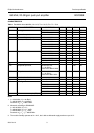
CHARACTERISTICS
Table 1 Bandwidth 40 to 860 MHz; V
B
= 24 V; T
mb
=30°C; Z
S
=Z
L
=75Ω
Notes
1. f
p
= 55.25 MHz; V
p
= 44 dBmV;
f
q
= 805.25 MHz; V
q
= 44 dBmV;
measured at f
p
+f
q
= 860.5 MHz.
2. Measured according to DIN45004B:
f
p
= 851.25 MHz; V
p
=V
o
;
f
q
= 858.25 MHz; V
q
=V
o
−6 dB;
f
r
= 860.25 MHz; V
r
=V
o
−6 dB;
measured at f
p
+f
q
−f
r
= 849.25 MHz.
3. The module normally operates at V
B
= 24 V, but is able to withstand supply transients up to 30 V.
SYMBOL PARAMETER CONDITIONS MIN. TYP. MAX. UNIT
G
p
power gain f = 50 MHz 19.5 − 20.5 dB
f = 860 MHz 20 −−dB
SL slope cable equivalent f = 40 to 860 MHz 0 − 2dB
FL flatness of frequency response f = 40 to 860 MHz −−±0.3 dB
s
11
input return losses f = 40 to 80 MHz 20 −−dB
f = 80 to 160 MHz 18.5 −−dB
f = 160 to 320 MHz 17 −−dB
f = 320 to 640 MHz 15.5 −−dB
f = 640 to 860 MHz 14 −−dB
s
22
output return losses f = 40 to 80 MHz 20 −−dB
f = 80 to 160 MHz 18.5 −−dB
f = 160 to 320 MHz 17 −−dB
f = 320 to 640 MHz 15.5 −−dB
f = 640 to 860 MHz 14 −−dB
s
21
phase response f = 50 MHz −45 − +45 deg
CTB composite triple beat 49 channels flat;
V
o
= 44 dBmV;
measured at 859.25 MHz
−−−60 dB
CSO composite second order distortion 49 channels flat;
V
o
= 44 dBmV;
measured at 860.5 MHz
−−−60 dB
d
2
second order distortion note 1 −−−68 dB
V
o
output voltage d
im
= −60 dB; note 2 57.5 59 − dBmV
NF noise figure f = 50 MHz −−5dB
f = 550 MHz −−5.5 dB
f = 650 MHz −−6.5 dB
f = 750 MHz −−6.5 dB
f = 860 MHz −−7.5 dB
I
tot
total current consumption (DC) note 3 −−235 mA