


2001 Nov 15 3
Philips Semiconductors Productspecification
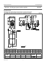
550 MHz, 18.5 dB gain power doubler amplifier BGD502
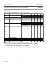
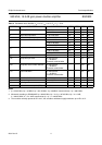
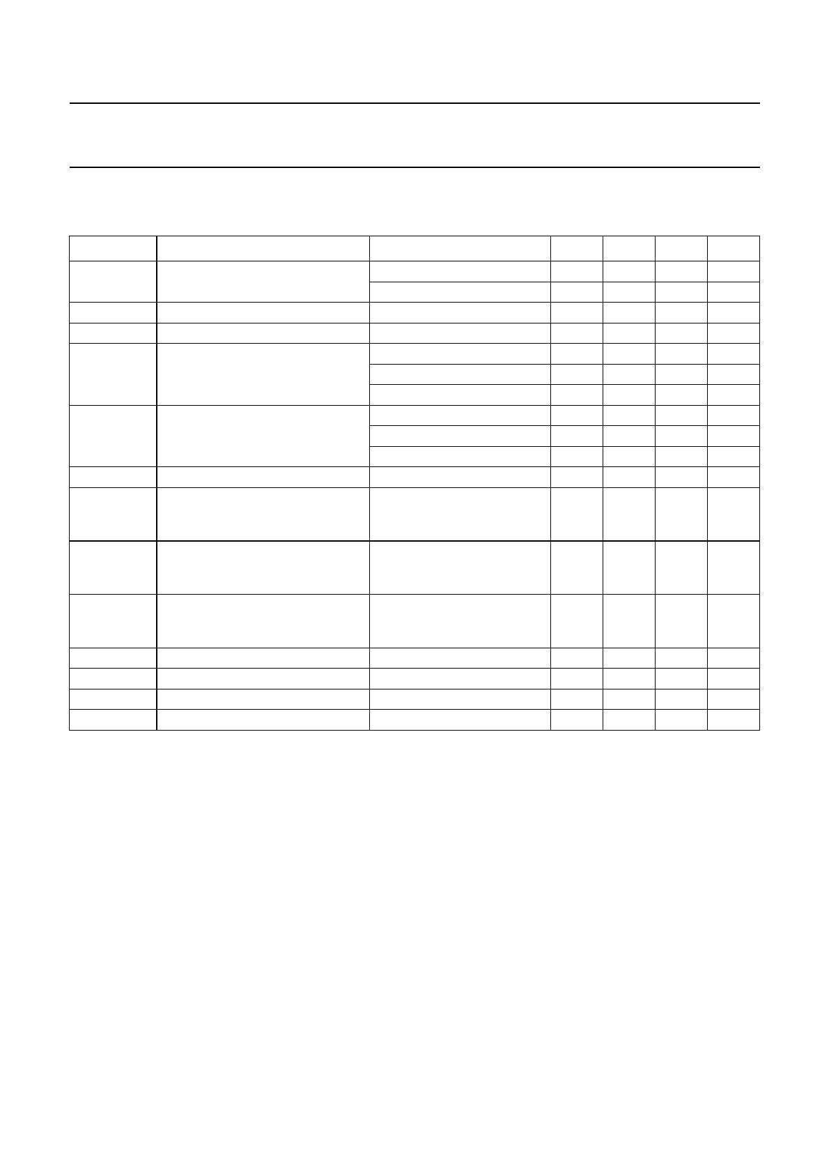
CHARACTERISTICS
Table 1 Bandwidth 40 to 550 MHz; V
B
= 24 V; T
mb
=35°C; Z
S
=Z
L
=75Ω.
Notes
1. fp = 55.25 MHz; Vp = 44 dBmV; fq = 493.25 MHz; Vq = 44 dBmV; measured at fp + fq = 548.5 MHz.
2. Measured according to DIN45004B: fp = 540.25 MHz; Vp = Vo; fq = 547.25 MHz; Vq = Vo −6 dB;
fr = 549.25 MHz; Vr = Vo −6 dB; measured at fp + fq − fr = 538.25 MHz.
3. The module normally operates at VB = 24 V, but are able to withstand supply transients up to VB = 30 V.
SYMBOL PARAMETER CONDITIONS MIN. TYP. MAX. UNIT
G
p
power gain f = 50 MHz 18 − 19 dB
f = 550 MHz 18.8 − 20.8 dB
SL slope cable equivalent f = 40 to 550 MHz 0.2 − 2.2 dB
FL flatness of frequency response f = 40 to 550 MHz −−±0.3 dB
s
11
input return losses f = 40 to 80 MHz 20 −−dB
f = 80 to 160 MHz 19 −−dB
f = 160 to 550 MHz 18 −−dB
s
22
output return losses f = 40 to 80 MHz 20 −−dB
f = 80 to 160 MHz 19 −−dB
f = 160 to 550 MHz 18 −−dB
s
21
phase response f = 50 MHz +135 − +225 deg
CTB composite triple beat 77 channels flat;
V
o
= 44 dBmV;
measured at 547.25 MHz
−−−65 dB
X
mod
cross modulation 77 channels flat;
V
o
= 44 dBmV;
measured at 55.25 MHz
−−−68 dB
CSO composite second order distortion 77 channels flat;
V
o
= 44 dBmV;
measured at 548.5 MHz
−−−62 dB
d
2
second order distortion note 1 −−−72 dB
V
o
output voltage d
im
= −60 dB; note 2 64 −−dBmV
NF noise figure f = 550 MHz −−8dB
I
tot
total current consumption (DC) note 3 − 415 435 mA