


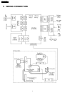
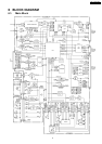
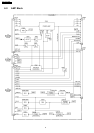
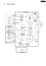
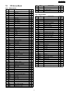
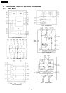
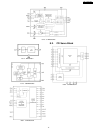
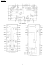
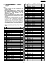
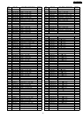
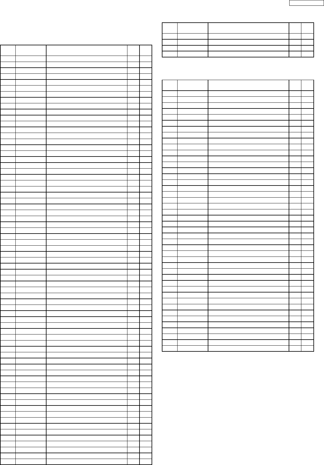
7.2. CD Servo Block
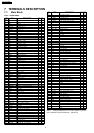
IC402 : MN662783RPW
Pin
No.
Port Descriptions I/O Vol.
(V)
1 VDD +5V power supply - 5.0
2 D0 D-RAM data I/O 2.3
3 D1 D-RAM data I/O 1.8
4 NWE D-RAM data write O 4.9
5 NRAS D-RAM row address strobe O 3.4
6 D2 D-RAM data I/O 0.8
7 D3 D-RAM data I/O 0
8 NCAS0 D-RAM columun address strobe O 3.9
9 A10 D-RAM address O 3.9
10 A8 D-RAM address O 0.6
11 A7 D-RAM address O 1.1
12 A6 D-RAM address O 0.7
13 A5 D-RAM address O 0
14 A4 D-RAM address O 1.1
15 A9 D-RAM address O 0.4
16-18 A0 D-RAM address O 1.0
19 A3 D-RAM address O 0
20 DVSS Ground - 0
21 DVDD +5V power supply - 5.0
22,23 - Not used - -
24 TVD Traverse motor control O 2.5
25 PC Not used - -
26 ECS Spindle motor control O 2.4
27 TRD Tracking coil drive O 2.5
28 FOD Focus coil drive O 2.4
29 FBAL Focus balance O 1.9
30 TBAL Tracking balance O 3.0
31 VREF Refence voltage I 2.5
32 FE Focus error I 2.5
33 TE Tracking error I 2.5
34 RFENV RF envelope I 2.5
35 OFTR Off track signal I 0
36 /RFDET RF detecting signal I 0
37 BDO Drop-out signal I 0
38 LDON Laser on signal O 4.5
39 ARF RF signal I 2.5
40 IREF Reference current input I 1.2
41 DRF Bias for DSL I 2.4
42 DSLF Loop filter for DSL I/O 2.5
43 DSLF2 Loop filter for DSL I/O 2.2
44 PLLF Loop filter for PLL I/O 1.4
45 VCOF Not used - -
46 AVDD +5V power supply - 5.0
47 AVSS Ground - 0
48 OUTL L channel output O 2.3
49 AVSS Ground - 0
50 OUTR R channel output O 2.3
51 AVDD +5V power supply - 4.7
52-54 - (Connecting to ground) - 0
55 FLAG Flag output O 0
56 FCLK Frame clock O 0
57-59 - Not used - -
60 TX Not used - -
61 MCLK Clock for I/F command I 1.0
62 MDATA Date for I/F command I 3.1
63 MLD I/F command load I 5.0
64 BLKCK Subcode block clock O 0
65 SQCK Ext.clock for sub code-Q I 5.0
66 SUBQ Code for sub. code-Q O 3.8
67 DMUTE Mute input I 0
68 STAT Status signal O 5.0
69 NRST Reset input I 5.0
70 CSEL (Connecting to ground) - 0
71 PMCK Clock output O 2.5
72 SMCK Clock output O 2.5
73 SUBC Serial data of sub code O 0
74 SBCK Shift clock for SUBC I 0.6
75 NCLDCK Not used - -
76 NTEST (Connecting to VDD) - 5.0
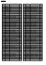
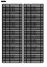
Pin
No.
Port Descriptions I/O Vol.
(V)
77 X1 Crystal oscillator - 0.4
78 X2 Crystal oscillator - 3.2
79 DVDD +5V power supply - 5.0
80 DVSS Ground - 0
IC401 : MN101C30AAE
Pin
No.
Port Descriptions I/O Vol.
(V)
1 SW4 Disc clamp detection I 0
2 SW5 Inner track detection I 5.0
3 SW2 Feeder arm detection I 4.8
4 PAG (Connecting to ground) - 0
5 IFR (Connecting to ground) - 0
6 VREF+ +5V power supply - 5.0
7 VDD +5V power supply - 5.0
8 OSC2 Crystal oscillator - 2.2
9 OSC1 Crystal oscillator - 2.1
10 VSS Ground - 0
11 XI (Connecting to ground) - 0
12 XO Not used - -
13 GND Ground - 0
14 SOMI CD changer serial data O 4.3
15 SIMO CD changer serial data I 1.3
16 SCKM Clock for serial data I 5.0
17 SB01 Not used - -
18 SUBQ Code for sub. code-Q I 1.6
19 SQCK Ext. clock for sub. code-Q O 5.0
20 P0G Not used - -
21 RST Reset input I 4.9
22 BD0 Drop-out signal I 0
23 PC1 Loading motor driver control O 5.0
24-26 - Not used - -
27 CDON CD activity I 5.0
28 BLKCK Subcode block clock O 0
29-31 - Not used - -
32 PC2 Focus/Tracking driver control O 0
33-36 - Not used - -
37 LOD Loading motor control I/O 2.5
38 TRV Traverse motor control I/O 2.4
39 NRST Servo IC reset O 5.0
40 STAT Status signal I 2.1
41 DMUTE DSP mute O 0
42-55 - Not used - -
56 MASHON Servo IC OSC control O 0.2
57 MCLK Command clock O 4.1
58 MDATA Command data O 3.1
59 MLD Command load O 5.0
60 P80 Not used - -
61 VREF- (Connecting to ground) - 0
62 Q1 Photo sensor signal (DISC IN) I 4.5
63 Q3 Photo sensor signal (DISC OUT) I 4.2
64 Q6 Photo sensor signal (Option) I 5.0
9
V.W. / CQ-JV1060L