


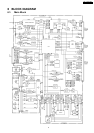
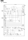
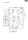
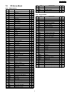
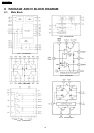
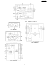
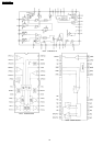
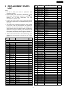
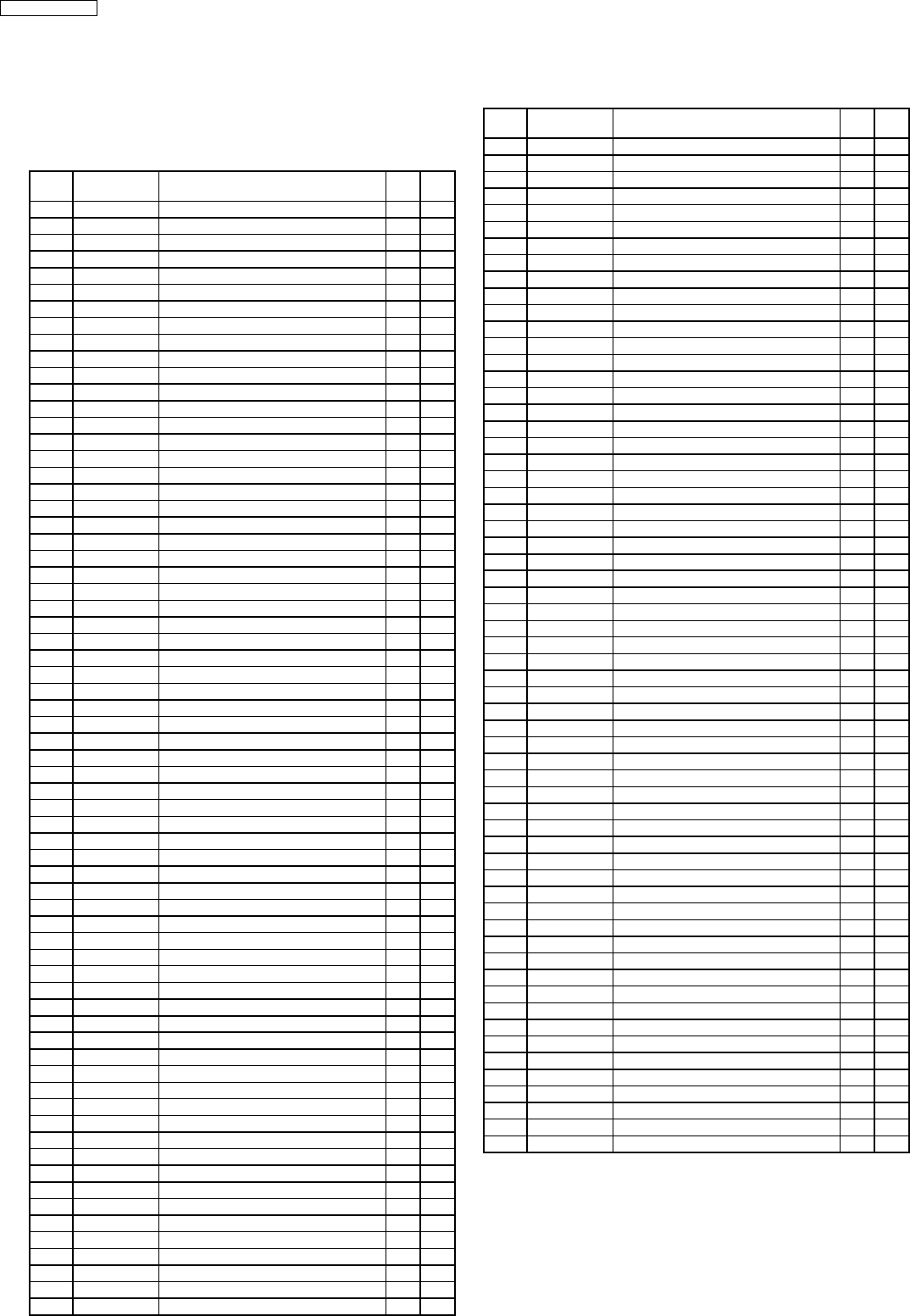
7.1. Main Block
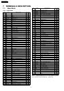
IC701 : C2CBKA00001
Pin
No.
Port Descriptions I/O Vol.
(V)
1 RSTOUT Not used - -
2 NMI (VDD pull-up) - 4.8
3 VSS Ground - 0
4 VDD +5V power supply - 4.8
5 LCD.ADR LCD addrress O 0
6 CD.SW3 CD disc out I 4.4
7 CD.SW1 CD disc in I 4.5
8 P.ON System power on O 4.8
9 CAN6.1V Battery level detection (6.1V) I 4.7
10 SAFE Safety LED control O 4.8
11 ILL2 Illumi. on (LCD) O 4.8
12 ILL Illumi. on (Button) O 4.8
13 KI0 Key data input I 0
14 KI1 Key data input I 0
15 KI2 Key data input I 0
16 KI3 Key data input I 0
17 VSS Ground - 0
18 VDD +5V power supply - 4.8
19 SR.DATA Serial data I/O 4.8
20 SR.CLK Clock for serial data O 4.8
21 ANT.CNT ANT1 amp power control O 0
22 A/B.IN Tape side detection I 4.7
23 TUN.A Tuning/Scan SW I 0
24 TUN.B Tuning/Scan SW I 0
25 VSS Ground - 0
26 VDD +5V power supply - 4.8
27 DEV FM deviation I 0
28 ADJ FM adjacent interference I 0
29 M.P FM multipath interference I 0
30 FILD Fieldstrength level I 0.5
31 IF.V ANT2 current intensity I 0.5
32 ANT.V ANT1 current intensity I 0.5
33 BATT.V Battery level detection I 2.6
34 FAD Fader level I 2.3
35 VA.REF +5V power supply - 4.8
36 VA.GND Ground - 0
37 BAL Balance level I 2.3
38 TRE Treble level I 0
39 MID Middle level I 1.0
40 BASS Bass level I 1.0
41 VSS Ground - 0
42 VDD +5V power supply - 4.8
43 BAT.DET Battery level detection I 4.8
44 CC.EJ Tape eject I 4.8
45 CD.EJ CD eject I 1.8
46 ALARM Alarm signal I 0
47 P.SW Power on SW I 4.8
48 CD.SW2 CD SW2 input I 0
49 T.LOAD Tape loading detection I 0
50 DIAG.CONT Not used - -
51 VSS Ground - 0
52 VDD +5V power supply - 4.8
53 IF.ON ANT2 amp power control O 0
54 RADIO.ON Radio power control O 4.8
55 DSP.DET DSP in activity I 4.8
56 CD.RST CD reset O 4.8
57 CD.SIM0 CD serial data O 0
58 CD.ON CD controller enable O 0
59 BIT3 Tape mode SW I 0
60 BIT2 Tape mode SW I 0
61 CDC.REMO CD.CH remocon data O 0
62 CDC.DATA CD.CH data I 0
63 BIT1 Tape mode SW I 0
64 EQ Metal tape detection I
65 MS MS detection I 0
66 CDC.CLK Shift clock for CD.CH data O 0
67 LCD.DET LCD driver in activity I 0
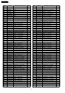
Pin
No.
Port Descriptions I/O Vol.
(V)
68 VDD +5V power supply - 4.8
69 VSS Ground - 0
70 CD.SOMI CD serial data I 0
71 /T.MUT Telephon mute I 0
72 CD.SCKM Shift clock for CD data O 0
73 CAN.EN CAN BUS enable O 0
74 CAN.STB CAN BUS strobe O 0
75 CAN.RX CAN BUS data I 4.8
76 CAN.TX CAN BUS data O 4.8
77 CAN.N.ERR CAN BUS error I 4.8
78 VDD +5V power supply - 4.8
79 VSS Ground - 0
80 /RD Not used - -
81 /WR Not used - -
82 /READY Not used - -
83 ALE Not used - -
84 /EA (VDD pull-up) - 0
85 K00 Key scan O 1.2
86 K01 Key scan O 1.2
87 K02 Key scan O 0
88 K03 Key scan O 1.2
89 PL04 Not used - -
90 R.IN Tape reverse O 0
91 T.IN Tape-in detection I 0
92 ENDA Tape end detection I 0
93 VDD +5V power supply - 4.8
94 VSS Ground - 0
95 CD.ON10V CD power on (10V) O 4.6
96 M2F Main motor control O 4.8
97 CC.ON Tape power on O 0
98 ENDB Tape end detection I 0
99 GAIN Audio output level control O 4.8
100 CD.ON5V CD power on (5V) O 4.8
101 F.IN Tape forword O 0
102 LCD.ON LCD driver reset O 4.8
103 E2DATA Security data I 0
104 ST-BY Power amp stand-by O 4.8
105 DSP.RST DSP reset O 4.8
106 AMP.ON External AMP power on O 0
107 MUT Not used - 4.8
108 M2 Main motor control O 0
109 VOL.A Volume control signal I 0
110 VOL.B Volume control signal I 0
111 VDD +5V power supply - 4.8
112 VSS Ground - 0
113 E2CE Security ROM chip enable O 0
114 LCD/E2 DT LCD/Security data O 0
115 LCD/E2 CK Clock for LCD/Security data O 0
116 LCD CS2 LCD driver select O 0
117 F/E.STP Radio stopsignal input I 0.9
118 F/E.DATA Tuner control data O 0
119 F/E.ENA Tuner enable O 0
120 F/E.CLK Shift clock for control data O 0
121 VDD +5V power supply - 4.8
122 VSS Ground - 0
123 XTAL2 Crystal oscillator - 2.0
124 XTAL1 Crystal osdillator - 2.3
125 VSS Ground - 0
126 XTAL3 Crystal oscillator - 2.3
127 XTAL4 Crystal oscillator - 2.3
128 RST Reset I 4.9
Note 1 : Voltage measuerments are with respect to ground,
with a voltmeter (internal resistance : 10M ohms).
7 TERMINALS DESCRIPTION
8
V.W. / CQ-JV1060L