


TDA8932B_3 © NXP B.V. 21 June 2007. All rights reserved.
Product data sheet Rev. 03— 21 June 2007 6 of 48
NXP Semiconductors
TDA8932B
Class-D audio amplifier
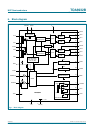
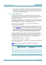
8.2 Mode selection and interfacing
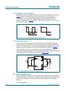
The TDA8932B can be switched in three operating modes using pins POWERUP and
ENGAGE:
• Sleep mode: with low supply current.
• Mute mode: the amplifiers are switching idle (50 % duty cycle), but the audio signal at
the output is suppressed by disabling the Vl-converter input stages. The capacitors on
pins HVP1 and HVP2 have been charged to half the supply voltage (asymmetrical
supply only).
• Operating mode: the amplifiers are fully operational with output signal.
• Fault mode.
Both pins POWERUP and ENGAGE refer to pin CGND.
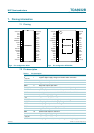
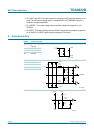
Table 4 shows the different modes as a function of the voltages on the POWERUP and
ENGAGE pins.
[1] In case of symmetrical supply conditions the voltage applied to pins POWERUP and ENGAGE must never
exceed the supply voltage (V
DDA
, V
DDP1
or V
DDP2
).
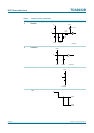
If the transition between Mute mode and Operating mode is controlled via a time constant,
the start-up will be pop free since the DC output offset voltage is applied gradually to the
output between Mute mode and Operating mode. The bias current setting of the
VI-converters is related to the voltage on pin ENGAGE:
• Mute mode: the bias current setting of the VI-converters is zero (VI-converters
disabled)
• Operating mode: the bias current is at maximum
The time constant required to apply the DC output offset voltage gradually between Mute
mode and Operating mode can be generated by applying a decoupling capacitor on pin
ENGAGE. The value of the capacitor on pin ENGAGE should be 470 nF.
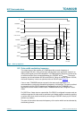
Table 4. Mode selection
Mode Pin
POWERUP ENGAGE DIAG
Sleep < 0.8 V < 0.8 V don’t care
Mute 2 V to 6.0 V
[1]
< 0.8 V
[1]
> 2 V
Operating 2 V to 6.0 V
[1]
2.4 V to 6.0 V
[1]
>2V
Fault 2 V to 6.0 V
[1]
don’t care < 0.8 V