


TDA8932B_3 © NXP B.V. 21 June 2007. All rights reserved.
Product data sheet Rev. 03— 21 June 2007 5 of 48
NXP Semiconductors
TDA8932B
Class-D audio amplifier
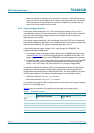
[1] The exposed die pad has to be connected to V
SSD(HW)
.
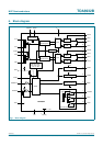
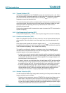
8. Functional description
8.1 General
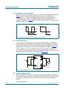
The TDA8932B is a mono full-bridge or stereo half-bridge audio power amplifier using
class-D technology. The audio input signal is converted into a Pulse Width Modulated
(PWM) signal via an analog input stage and PWM modulator. To enable the output power
Diffusion Metal Oxide Semiconductor (DMOS) transistors to be driven, this digital PWM
signal is applied to a control and handshake block and driver circuits for both the high side
and low side. A 2nd-order low-pass filter converts the PWM signal to an analog audio
signal across the loudspeakers.
The TDA8932B contains two independent half-bridges with full differential input stages.
The loudspeakers can be connected in the following configurations:
• Mono full-bridge: Bridge Tied Load (BTL)
• Stereo half-bridge: Single-Ended (SE)
The TDA8932B contains common circuits to both channels such as the oscillator, all
reference sources, the mode functionality and a digital timing manager. The following
protections are built-in: thermal foldback, temperature, current and voltage protections.
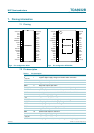
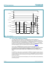
HVP2 19 half supply output voltage 2 for charging single-ended capacitor for
channel 2
V
DDP2
20 positive power supply voltage for channel 2
BOOT2 21 bootstrap high-side driver channel 2
OUT2 22 PWM output channel 2
V
SSP2
23 negative power supply voltage for channel 2
STAB2 24 decoupling of internal 11 V regulator for channel 2 drivers
STAB1 25 decoupling of internal 11 V regulator for channel 1 drivers
V
SSP1
26 negative power supply voltage for channel 1
OUT1 27 PWM output channel 1
BOOT1 28 bootstrap high-side driver channel 1
V
DDP1
29 positive power supply voltage for channel 1
HVP1 30 half supply output voltage 1 for charging single-ended capacitor for
channel 1
OSCIO 31 oscillator input in slave configuration or oscillator output in master
configuration
V
SSD(HW)
32 negative digital supply voltage and handle wafer connection
Exposed die
pad
- HTSSOP32 package only
[1]
Table 3. Pin description (Continued)
Symbol Pin Description