


MAX9777/MAX9778
Stereo 3W Audio Power Amplifiers with
Headphone Drive and Input Mux
____________________________________________________________________________________________________________________________________________________________________________
19
Component Selection
Gain-Setting Resistors
External feedback components set the gain of the
MAX9777/MAX9778. Resistor R
IN
sets the gain of the
input amplifier (A
VIN
), and resistor R
F
sets the gain of
the second stage amplifier (A
VOUT
):
Combining A
VIN
and A
VOUT
, R
IN
and R
F
set the single-
ended gain of the device as follows:
As shown, the two-stage amplifier architecture results
in a noninverting gain configuration, preserving
absolute phase through the MAX9777/MAX9778. The
gain of the device in BTL mode is twice that of the sin-
gle-ended mode. Choose R
IN
between 10kΩ and 15kΩ
and R
F
between 15kΩ and 100kΩ.
Input Filter
The input capacitor (C
IN
), in conjunction with R
IN
, forms
a highpass filter that removes the DC bias from an
incoming signal. The AC-coupling capacitor allows the
amplifier to bias the signal to an optimum DC level.
Assuming zero-source impedance, the -3dB point of
the highpass filter is given by:
Choose R
IN
according to the
Gain-Setting Resistors
sec-
tion. Choose the C
IN
such that f
-3dB
is well below the
lowest frequency of interest. Setting f
-3dB
too high affects
the amplifier’s low-frequency response. Use capacitors
whose dielectrics have low-voltage coefficients, such as
tantalum or aluminum electrolytic. Capacitors with high-
voltage coefficients, such as ceramics, may result in an
increased distortion at low frequencies.
Other considerations when designing the input filter
include the constraints of the overall system,
the actual frequency band of interest, and click-and-
pop suppression.
Output-Coupling Capacitor
The MAX9777/MAX9778 require output-coupling
capacitors to operate in single-ended (headphone)
mode. The output-coupling capacitor blocks the DC
component of the amplifier output, preventing DC cur-
rent from flowing to the load. The output capacitor and
the load impedance form a highpass filter with a -3dB
point determined by:
As with the input capacitor, choose C
OUT
such that
f
-3dB
is well below the lowest frequency of interest.
Setting f
-3dB
too high affects the amplifier‘s low-fre-
quency response.
Load impedance is a concern when choosing C
OUT
.
Load impedance can vary, changing the -3dB point of
the output filter. A lower impedance increases the cor-
ner frequency, degrading low-frequency response.
Select C
OUT
such that the worst-case load/C
OUT
com-
bination yields an adequate response. Select capaci-
tors with low ESR to minimize resistive losses and
optimize power transfer to the load.
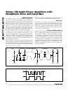
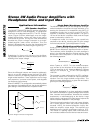
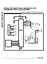
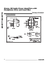
If layout constraints require a physically smaller output-
coupling capacitor, decrease the value of C
OUT
and add
series resistance to the output of the MAX9777/MAX9778
(see Figure 9). With the added series resistance at the
output, the cutoff frequency of the highpass filter is:
Since the cutoff frequency of the output highpass filter
is inversely proportional to the product of the total load
resistance seen by the outputs (R
L
+ R
SERIES
) and
C
OUT
, increase the total resistance seen by the
MAX9777/MAX9778 outputs by the same amount C
OUT
is decreased to maintain low-frequency performance.
Since the added series resistance forms a voltage-
divider with the headphone speaker resistance for fre-
quencies within the passband of the highpass filter,
there is a loss in voltage gain. To compensate for this
loss, increase the voltage gain setting by an amount
equal to the attenuation due to the added series resis-
tance. Use the following equation to approximate the
required voltage gain compensation:
A
RR
R
V COMP
L SERIES
L
_
log=
+
⎛
⎝
⎜
⎞
⎠
⎟
20
f
RR C
dB
L SERIES OUT
−
=
+
()
3
1
2π
f
RC
dB
L OUT
−
=
3
1
2π
f
RC
dB
IN IN
−
=
3
1
2π
AA A
k
R
R
k
R
R
V VIN VOUT
IN
FF
IN
=× =−
⎛
⎝
⎜
⎞
⎠
⎟
×−
⎛
⎝
⎜
⎞
⎠
⎟
=+
⎛
⎝
⎜
⎞
⎠
⎟
10
10
Ω
Ω
A
k
R
A
R
k
VIN
IN
VOUT
F
=−
⎛
⎝
⎜
⎞
⎠
⎟
=−
⎛
⎝
⎜
⎞
⎠
⎟
10
10
Ω
Ω
,
C
OUT
R
SERIES
R
L
OUT_+
Figure 9. Reducing C
OUT
by Adding R
SERIES