


b15 b14 b13 b12 b11 b10 b9 b8 b7 b6 b5 b4 b3 b2 b1 b0
CH6 CH5 CH4 CH3 CH2 CH1
#33 H 40E9
○
R/W Reset to factory
setting and set
characteristics
adjustable priority
Example: Setting of CH1
1. When b0=0, user can set OFFSET and GAIN value of CH1 (CR#18, CR#24).
When b0=1, inhibit user to adjust OFFSET and GAIN value of CH1 (CR#18,
CR#24).
2. b1 means if characteristic register is latched. b1=0 (factory setting, latched), b1=1
(not latched).
3. b2: Set to 1 and PLC will be reset to factory settings.
The setting of CH5~CH6, give CH5 setting for example:
b13, b12:
00: can be adjusted, latched.
01: can be adjusted, non-latched.
10: inhibit adjust.
11: reset to factory settings and clear b12, b13 to 0.
#34 H 40EA
○
R Software version Display software version in hexadecimal. Example: H 010A = version 1.0A.
#35~#48 System used
○ means latched.
╳ means non-latched.
R means can read data by using FROM command or RS-485.
W means can write data by using TO command or RS-485.
LSB (Least Significant Bit): 1. Voltage input: 1
LSB
=10V/2000=5mV. 2. Current input: 1
LSB
=20mA/1000=20µA.
3. Voltage output: 1
LSB
=10V/4000=2.5mV. 4. Current output: 1
LSB
=20mA/4000=5µA.
Explanation:
1. CR#0: The PLC model type.
2. CR#1: b11~b0 are used to set 4 internal channels working mode of analog input module (AD).
b12~b15 are used to set 2 channels working mode of analog output module (DA). Every channel
has four modes that can be set individually. For example: if setting CH1 to mode 0 (b2~b0=000),
CH2 to mode 1(b5~b3=001), CH3: mode2 (b8~b6=010), CH4: mode 3(b11~b9=011), b0~b11
need be set to H688. If setting CH5: mode 2 (b13~b12=10), CH6: mode 1 (b15~b14=01),
b12~b15 need be set to H5. The factory setting is H0000.
3. CR#2 ~ CR#5: Used to set the number of piece of input readings for the average temperature
calculation. The available range is K1~K4096 and factory setting is K10.
4. CR#6 to CR#9: The average value of temperature in ℃. Temperature is calculated by averaging
multiple temperature readings. Example: If CR#2 is 10, the temperature in CR#6 will be the
average of the last 10 readings on CH1.
5. CR#10 ~ CR#11 are used to set the output value of CH5 and CH6. The setting range is
K0~K4000. The factory setting is K0 and unit is LSB.
6. CR#12 ~ CR#15: used to save the present value of input signal of CH1~CH4.
7. CR#16, CR#17, CR#28, CR#29 are reserved.
8. CR #18~ CR #21: used to adjust the OFFSET value of CH1~CH4 if analog input either in voltage
or in current is 0 after it converts from analog to digital. Voltage setting range:
-5V~+5V(-1000
LSB
~+1000
LSB
). Current setting range: -20mA~+20mA (-1000
LSB
~+1000
LSB
).
9. CR #22~ CR #23: used to adjust the OFFSET value of CH5~CH6 if analog input either in voltage
or in current is 0 after it converts to digital. Factory setting is K0, and the unit is
LSB
. The setting
range is -2000~+2000. Voltage setting range: -5V~+5V(-2000
LSB
~+2000
LSB
). Current setting
range: -10mA~+10mA (-2000
LSB
~+2000
LSB
).
10. CR #24~ CR #27: used to adjust the GAIN value of CH1~CH4. The value of analog input either
in voltage or in current after it was converted to digital based upon full scale of 4000. Voltage
setting range: -4V~+20V(-800
LSB
~+4000
LSB
). Current setting range: -16mA~+52mA (-800
LSB
~+2600
LSB
). But it needs to notice that GAIN VALUE - OFFSET VALUE = +200
LSB
~+3000
LSB
(voltage) or +200
LSB
~+1600
LSB
(current). If the value difference comes up small (within range),
the output signal resolution is then slim and the variation is definitely larger. On the contrast, if
the value difference exceeds the range, the output signal resolution becomes larger and the
variation is definitely smaller.
11. CR #28~ CR #29: used to adjust the GAIN value of CH5~CH6. The value of analog input either
in voltage or in current after it converts to digital based upon full scale of 2000. Voltage setting
range: -4V~+20V(-1600
LSB
~+8000
LSB
). Current setting range: -8mA ~+40mA (-1600
LSB
~+8000
LSB
).
Please be noticed that GAIN VALUE – OFFSET VALUE = +400
LSB
~+6000
LSB
(voltage or current).
If the value difference comes up small (within range), the output signal resolution is then slim
and the variation is definitely larger. On the contrast, if the value difference exceeds the range,
the output signal resolution becomes larger and the variation is definitely smaller.
12. CR#30 is the fault code. Please refer to the chart below.
Fault description Content b15~b8 B7 b6 b5 b4 b3 b2 b1 b0
Power source abnormal
(Low voltage alarm)
K1(H1) 0 0 0 0 0 0 0 1
User setting D/A output
exceeds range
K2(H2) 0 0 0 0 0 0 1 0
Setting mode error K4(H4) 0 0 0 0 0 1 0 0
Offset/Gain error K8(H8) 0 0 0 0 1 0 0 0
Hardware malfunction K16(H10) 0 0 0 1 0 0 0 0
Digital range error K32(H20) 0 0 1 0 0 0 0 0
Average times setting error K64(H40) 0 1 0 0 0 0 0 0
Command error K128(H80)
Reserved
1 0 0 0 0 0 0 0
Note: Each fault code will have corresponding bit (b0~b7). Two or more faults may happen at the same time. 0 means
normal and 1 means having fault.
13. CR#31: RS-485 communication address. Setting range is 01~255 and factory setting is K1.
14. CR#32: RS-485 communication baud rate: 4800, 9600, 19200, 38400, 57600 and 115200.
b0:4800bps, b1:9600bps (factory setting), b2:19200bps, b3:38400 bps, b4:57600 bps,
b5:115200 bps, b6~b13: Reserved, b14: switch between low bit and high bit of CRC code (RTU
mode only) b15: ASCII / RTU mode. For ASCII mode, date format is 7Bits, even, 1 stop bit (7 E
1). For RTU mode, date format is 8Bits, even, 1 stop bit (8 E 1).
15. CR#33 is used to set the internal function priority. For example: characteristic register. Output
latched function will save output setting in the internal memory before power loss.
16. CR#34: software version.
17. CR#35~ CR#48: system used.
18. The corresponding parameters address H 40C8~H 40F9 of CR#0~CR#48 will allow user to
read/write data via RS-485.
A. Baud rate can be 4800, 9600, 19200, 38400, 57600, 115200bps.
B. MODBUS communication protocol can be either in ASCII or in RTU mode. For ASCII mode,
date format is 7Bits, even, 1 stop bit (7 E 1). For RTU mode, date format is 8Bits, even, 1
stop bit (8 E 1).
C. Function code: 03H read data from register.
06H write one WORD into register.
10H write multiple WORD into register.
5
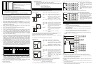
Adjust A/D Conversion Characteristic Curve
5.1 Adjust A/D Conversion Characteristic Curve of CH1~CH4
Voltage input mode
Mode 0 of CR#1: GAIN=5V(1000
LSB
), OFFSET=0V (0
LSB
).
Mode 1 of CR#1: GAIN=6V(1200
LSB
), OFFSET=2V (400
LSB
).
GAIN:
Voltage input value when digital output is 4000.
Setting range is -4V~+20V(-800
LSB
~ +4000
LSB
)
OFFSET:
Voltage input value when digital output is 0.
Setting range: -5V~+5V(-1000
LSB
~ +1000
LSB
)
+2000
+1000
-1000
10V
digital output
Voltage
input
-2000
-6V-10V
6V5V2V
0
Mode 1
Mode 0
GAIN
OFFSET
GAIN-OFFSET: Setting range is +1V~+15V (+200
LSB
~ +3000
LSB
)
Current input mode:
Mode 2 of CR#1: GAIN = 20mA(1000
LSB
), OFFSET=4mA (200
LSB
).
Mode 3 of CR#1: GAIN = 20mA(1000
LSB
), OFFSET=0mA (0
LSB
).
GAIN:
Current input value when digital output is +4000.
Setting range is -20 mA~+20mA (-1000
LSB
~
+1000
LSB
)
OFFSET:
Current input value when digital output value is
0. Setting range is-16mA ~+52mA (-800
LSB
~
+2600
LSB
)
+2000
Digital output
Current
Input
-2000
-12mA-20mA
4mA
0
Mode 2
Mode 3
OFFSET
20mA
GAIN
GAIN-OFFSET:
Setting range is +4mA ~ +32mA (200
LSB
~
+1600
LSB
)
Use the chart above to adjust A/D conversion characteristic curve of voltage input mode and current
input mode. Users can adjust conversion characteristic curve by changing OFFSET values
(CR#18~CR#21) and GAIN values (CR#24~CR#27) depend on application.
LSB (Least Significant Bit): 1. voltage input: 1
LSB
=10V/2000=5mV. 2. current input: 1
LSB
=20mA/1000=
20µA.
5.2 Adjust D/A Conversion Characteristic Curve of CH5~CH6
Voltage output mode
Mode 0 of CR#1: GAIN = 5V(2000
LSB
), OFFSET=0V (0
LSB
)
Mode 1 of CR#1: GAIN = 6V(2400
LSB
), OFFSET=2V (800
LSB
).
GAIN: Voltage output value when digital input is K2000.
Setting range is -4V~+20V(-1600
LSB
~+8000
LSB
).
OFFSET: Voltage output value when digital input is K0.
Setting range: -5V~+5V(-2000
LSB
~ +2000
LSB
).
0
+2000 +4000
2V
5V
6V
10V
OFFSET
GAIN
Voltage output
mode 1
mode 0
Digital
input
GAIN-OFFSET:
Setting range is +1V~+15V(+400
LSB
~ +6000
LSB
)
Current output mode:
Mode 2 of CR#1: GAIN = 12mA(2400
LSB
),OFFSET=4mA (800
LSB
).
Mode 3 of CR#1: GAIN = 10mA(2000
LSB
), OFFSET=0mA (0
LSB
).
GAIN: Current output value when digital input value is
K2000. Setting range is -8mA ~+40mA (-1600
LSB
~+8000
LSB
).
OFFSET: Current output value when digital input is K0.
Setting range is -10mA ~+10mA (-2000
LSB
~+2000
LSB
).
0
+2000 +4000
20mA
OFFSET
GAIN
12mA
10mA
4mA
Current output
Mode 2
Mode 3
Digital
input
GAIN-OFFSET:
Setting range is +2mA~+30mA (+400
LSB
~+6000
LSB
)
Use the chart above to adjust D/A conversion characteristic curve of voltage output mode and
current output mode. Users can adjust conversion characteristic curve by changing OFFSET values
(CR#14~CR#15) and GAIN values (CR#18~CR#19) depend on application.
LSB (Least Significant Bit): 1. voltage output: 1
LSB
=10V/4000=2.5mV.
2. current output: 1
LSB
=20mA/4000=5µA.
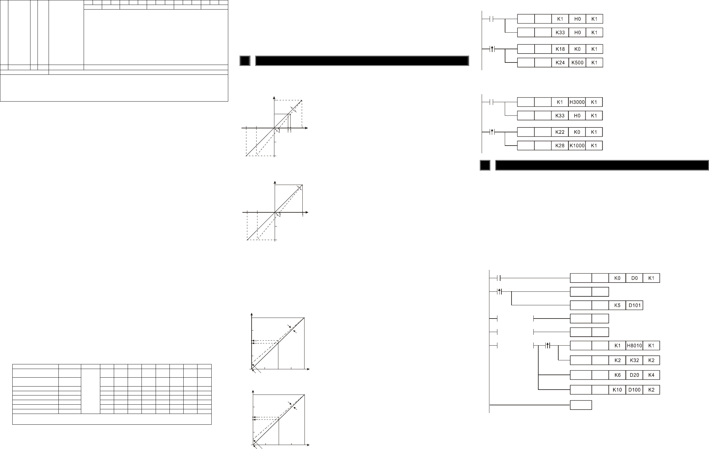
5.3 Program Example for Adjusting A/D Conversion Characteristics Curve
Example: setting OFFSET value of CH1 to 0V(=K0
LSB
) and GAIN value of CH1 to 2.5V(=K500
LSB
).
M1002
K0TO
K0TO
X0
K0TO
K0TO
Write H0 to CR#1 of analog input module
no. 0 and set CH1 to mode 0 (voltage input
-10V~+10V)
Write H0 to CR#33 and allow to adjust
characters of CH1.
When X0 switches from Off to On, K0
LSB
of
OFFSET value will be wrote in CR#18 and
K500
LSB
of GAIN value will be wrote in
CR#24.
5.4 Program Example for Adjusting D/A Conversion Characteristics Curve
Example: set OFFSET value of CH5 to 0V(=K0
LSB
) and GAIN value of CH1 to 2.5V(=K1000
LSB
).
M1002
K0TO
K0TO
X0
K0TO
K0TO
Write H3000 into CR#1 (b12~b15) of
analog input/output module#0. Setting CH5
to mode 3 (current output 0mA~ +20mA).
Write H0 into CR#33 (b12~b15) and allow
CH5, CH6 to adjust characteristics.
When X0 switches from Off to On, K0
LSB
of
OFFSET value will be wrote in CR#22 and
K1000
LSB
of GAIN value K1000
LSB
will be
wrote in CR#28.
6 Initial PLC Start-up
Lamp display:
1. Upon power-up, the ERROR LED will light for 0.5 seconds the POWER LED will light
continuously.
2. No errors= POWER LED on and ERROR LED off.
Low Voltage error (lower than 19.5V), ERROR LED will blink continuously till the power
supply rises above 19.5V.
3. DVP06XA-S connected to PLC MPU in series = RUN LED on MPU will be lit and A/D LED
or D/A LED should blink.
4. After receiving the first RS-485 command the A/D LED or D/A LED will blink.
5. If the input or output exceeds the upper or lower bounds, then the ERROR LED will blink.
6. When main CPU and expansion unit communicate time-out or abnormal interrupt, LED
ERROR of expansion unit will keep lighting.
Example:
M1000
FROM K0
INC D100
ADD D101
RST
TO K0
= K4000 D100
M1013
= K4000 D101
= HCC D0
RST
D100
D101
TO K0
FROM K0
TO K0
END
M1002
Explanation:
Reading the model type of expansion module K0 (should be HCC for DVP06XA-S model type).
If the model type is DVP06XA-S, set the input mode is (CH1, CH3, CH4)= mode 0, (CH2)= mode 2,
and set the output mode is (CH5)=mode 0, (CH6)=mode 2.
Setting the average number of CH1 and CH2 are K32.
Reading the input signal average value of CH1~CH4 (4 data) from CR#6~CR#9 and save in
D20~D23.
In each second, D100 will increase K1 and D101 will increase K5. When the value of D100 and
D101 are K4000, it will clear to 0.
Writing the output setting value of D100 and D101 into CR#10 and CR#11. The analog output value
of CH5~CH6 will change with the value of D100 and D101.