


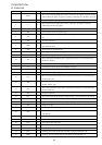
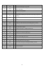
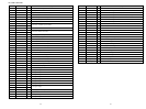
30
Pin No. Pin Name I/O Description
36
37
38
39, 40
41
42
43
44
45
46
47
48
49
50
51
52
53
54
55
56
57
58
59
60
61
62
63
64
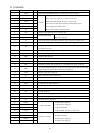
TES
HFL
SLOF
CV–, CV+
RFSM
RFS-
SLC
SLI
DGND
FSC
TBC
NC
DEF
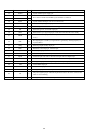
CLK
CL
DAT
CE
DRF
FSS
VCC2
REFI
VR
LF2
PH1
BH1
LDD
LDS
VCC1
O
O
I
I
O
I
O
I
—
O
I
—
O
I
I
I
I
O
I
—
—
O
I
I
I
O
I
—
Pin from which TES signal is output to DSP.
“High Frequency Level” is used to judge whether the main beam position is on top of
bit or on top of mirror.
Sled servo off control input pin.
CLV error signal input pin from DSP.
RF output pin.
RF gain setting and EFM signal 3T compensation constant setting pin together with
RFSM pin.
“Slice Level Control” is the output pin which controls the RF signal data slice level by
DSP.
Input pin which control the data slice level by the DSP.
Digital system GND.
Output pin to which external focus search smoothing capacitor is connected.
“Tracking Balance Control” EF balance variable range setting pin.
No connection.
Disc defect detector output pin.
Reference clock input pin. 4.23 MHz of the DSP is input.
Microprocessor command clock input pin.
Microprocessor command data input pin.
Microprocessor command chip enable input pin.
“Detect RF” RF level detector output.
“Focus Search Select” focus search mode (± search/+ search) select pin.
Servo system and digital system Vcc pin.
Pin to which external bypass capacitor for reference voltage is connected.
Reference voltage output pin.
Disc defect detector time constant setting pin.
Pin to which external capacitor for RF signal peak holding is connected.
Pin to which external capacitor for RF signal bottom holding is connected.
APC circuit output pin.
APC circuit input pin.
RF system Vcc pin.