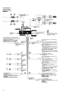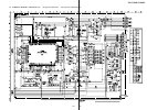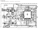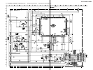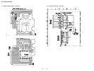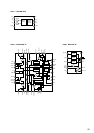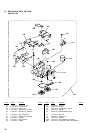
35
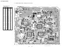
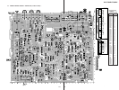
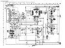
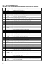
Pin No. Pin Name I/O Description
60 REDY O
Transfer enable signal output to the system controller (IC600)
“L”: transfer prohibition
61 TRDT O
Serial data output to the system controller (IC600) and liquid crystal display drive controller
(IC800)
62 XLAT I
Serial data latch pulse input from the system controller (IC600)
63 RVDT I
Serial data input from the system controller (IC600)
64 XS24 I
Serial data 24/32 bit slot selection signal input terminal
“L”: 24 bit slot, “H”: 32 bit slot (validity at slave mode) (fixed at “H” in this set)
65 VDD2 —
Power supply terminal (+3.3V) (digital system)
66 VSS3 —
Ground terminal (digital system)
67 to 69 SO1 to SO3 O
Serial data output terminal Not used (open)
70 SOUT O
Serial data output terminal Not used (open)
71 to 73 SI1 to SI3 I
Serial data input terminal Not used (fixed at “L”)
74 SIN I
Serial data input terminal Not used (fixed at “L”)
75 BCK I
Bit clock signal (2.8224 MHz) input terminal Not used (fixed at “H”)
76 LRCK I
L/R sampling clock signal (44.1 kHz) input terminal Not used (fixed at “H”)
77 XMST I
Bit clock (BCK) and L/R sampling clock (LRCK) signal master/slave mode selection signal input
terminal “L”: master mode, “H”: slave mode (fixed at “L” in this set)
78 VDD3 —
Power supply terminal (+3.3V) (digital system)
79 AVSP —
Ground terminal (PLL system)
80 XPLLEN I
PLL enable signal input terminal Normally: fixed at “L”
81 PLCLK O
PLL clock signal output terminal (22.5792 MHz)
82 XECKSTP I
PLL clock output control signal input terminal Not used (fixed at “L”)
83 AVDP —
Power supply terminal (+3.3V) (PLL system)
84 VSS4 —
Ground terminal (digital system)
85 to 94 T.P
I Input terminal for the test Normally: fixed at “L”
95 VDD4 —
Power supply terminal (+3.3V) (digital system)
96 AVSD —
Ground terminal (for D-RAM)
97 to 99 T.P
I Input terminal for the test Normally: fixed at “L”
100 AVDD —
Power supply terminal (+3.3V) (for D-RAM)