Description
1-2
Introduction and Description
1.1 Description
The THS4150 EVM is a good example of PCB design and layout for
high-speed operational amplifier applications. It is a complete circuit for the
high-speed operational amplifier. The EVM is made of the THS4150
high-speed operational amplifier, a number of passive components, and
various features and footprints that enable the user to experiment, test, and
verify various operational amplifier circuit implementations. The board
measures 4.5 inches in length by 2.5 inches in width.
Initially, this board is
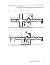
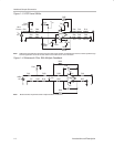
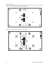
populated for a single-ended input amplifier (see Figure 1-2 for populated
circuits). The outputs (V
O+
and V
O–
) can be tested differentially or single
ended. Gain is set to one and can be changed by changing the ratios of the
feedback and gain resistors (see the device datasheet for recommended
resistor values). The user may populate various footprints on the evaluation
module board to verify filter designs or perform other experiments. Each input
is terminated with a 50-Ω resistor to provide correct line-impedance matching.
1.2 Evaluation Module Features
THS4150 high-speed operational amplifier EVM features include:
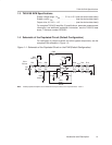
Voltage supply operation range: 5-V to ±15-V operation (see the
device data sheet)
Single and differential input and output capability
Nominal 50-Ω input and output termination resistors. They can be
configured according to the application requirement.
V
OCM
direct input control (see schematic and the device data sheet)
V
OCM
pin can be controlled via transformer center-tap (see
schematic)
Shutdown pin control, JU1 (if applicable to the device, see the device
data sheet)
Input and output transformer footprints for changing single-ended
signals to differential signals
Footprint for high-precision, balanced feedback and gain resistors
(0.01% or better)
Footprints for low-pass filter implementation (see application note
SLOA054A)
Footprints for antialiasing filter implementation (see application note
SLOA054A)
Differential probe terminals on input and output nodes for differential
probe insertion
Various GND and signal test points on the PCB
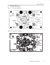
Circuit schematic printed on the back of the EVM
A good example of high-speed amplifier PCB design and layout


