


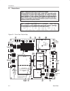
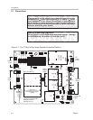
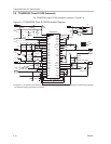
Plug-N-Play Platform Inputs and Outputs
3-5
Details
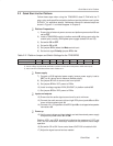
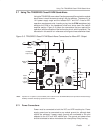
3.4 Control and Indicator Circuits
Three main control circuits are provided with the TPA032D03. The mute circuit
grounds the output of the active amplifier, the mode circuit selects between the
class-D amplifier and the headphone amplifier, and the shutdown circuit
places the entire device into a power-saving sleep mode to minimize current
consumption. Each of these inputs is TTL compatible: less than 0.8 V applied
to these pins is considered a logic low, and any voltage greater than 2 V is
considered a logic high.
Two indicator pins are also provided for feedback when an under-voltage or
thermal fault exists. Module pins are provided for easy connection of off-board
control and monitoring. There are two active low fault indicator pins on the
TPA032D03 amplifier IC (IC pins 41 and 42) that provide feedback when a fault
condition exists. Signals on these pins provide the status of the acvtive
amplifier: operational, thermal fault, and under-voltage lockout. Table 3–2 lists
the possible output conditions of these pins and a description of the fault
indicated.
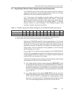
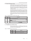
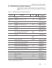
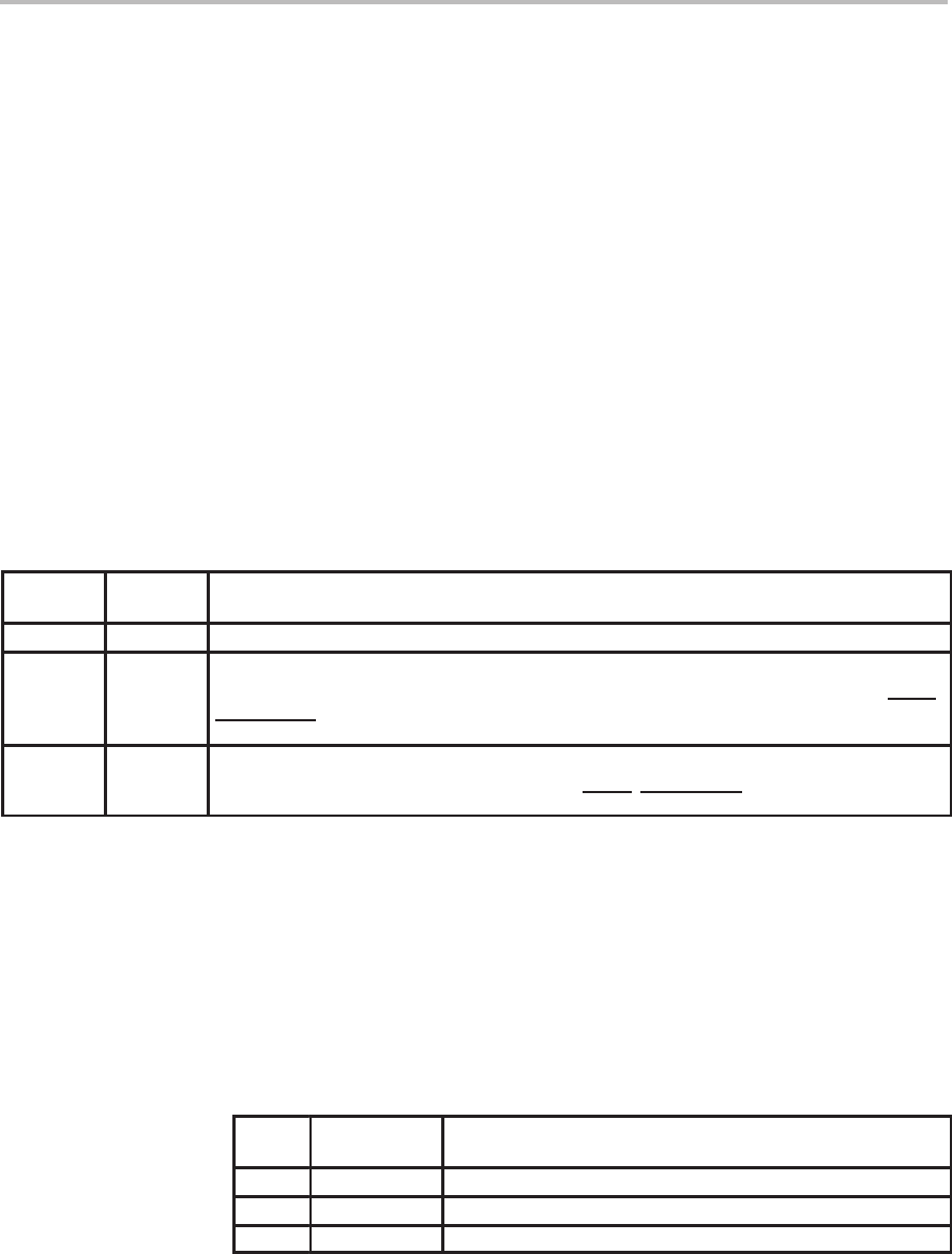
Table 3–2.TPA032D03 Class-D EVM Fault Indicator Table
FAULT 0
(TP 1)
FAULT 1
(TP 2)
DESCRIPTION
1 1 No fault. — The device is operating normally.
0 1 Charge pump under-voltage lockout (VCP-UV) fault. All low-side transistors are turned on, shorting
the load to ground. Normal operation resumes when the charge pump voltage is restored (not a
latched fault), however the Fault
indication
remains active until cleared by cycling MUTE,
SHUTDOWN
, or the power supply.
0 0 Thermal fault. All of the low-side transistors are turned on, shorting the load to ground. Once the
junction temperature drops by 20°C, normal operation resumes (not a latched fault). The Fault
indication
remains active until cleared by cycling MUTE, SHUTDOWN, or the power supply.
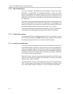
3.5 TPA032D03 Class-D EVM Test Points
Test points have been included on the TPA032D03 class-D EVM to facilitate
user analysis of device performance and design adjustments. Table 3–3 lists
each test point and its corresponding function.
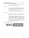
Table 3–3.TPA032D03 Class-D EVM Test Points
TEST
POINT
IC PIN or EVM
FUNCTION
FUNCTION
1 HPVCC Onboard 5-V supply
2 FAULT_1 MSB for logic-level fault output signal, open drain
3 FAULT_0 LSB for logic-level fault output signal, open drain