


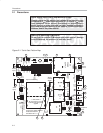

TPA2010D1 EVM PCB Layers
2-7
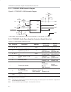
Operation
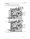
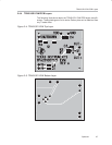
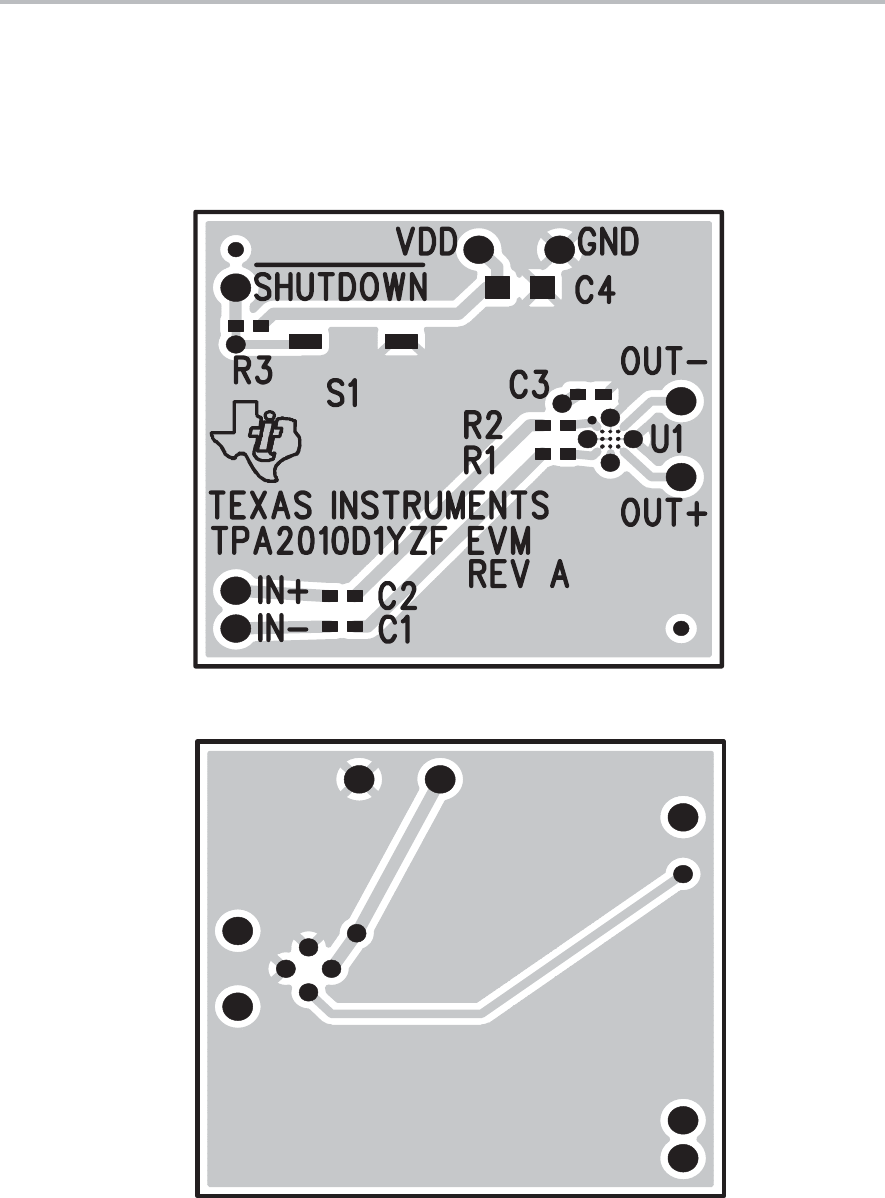
2.4.4 TPA2010D1 EVM PCB Layers
The following illustrations depict the TPA2010D1 EVM PCB layers and silk-
screen. These drawings are not to scale. Gerber plots can be obtained from
any TI sales office.
Figure 2−4. TPA2010D1 EVM Top Layer
Figure 2−5. TPA2010D1 EVM Bottom Layer