


26
XR-CA600/CA600V/CA600X
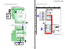
6-11. IC PIN FUNCTION DESCRIPTION
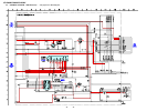
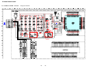
• MAIN BOARD IC501 MN101C49KTF (SYSTEM CONTROLLER)
Pin No. Pin Name I/O Description
1 VREF–
I
Reference voltage (0V) input terminal (for A/D converter)
2 VSM I
FM and AM signal meter voltage detection signal input from the FM/AM tuner unit (TU1)
(A/D input)
3 NIL I Not used (fixed at “L”)
4
KEYIN1
I
Key input terminal (A/D input) LSW902, LSW905 to LSW911, S902 to S905
(MENU, SOUND, ENTER, S SCROLL, PTY D DISPLAY, LIST, AF, TA, > M SEEK+,
. m SEEK–, DISC/PRESET+, DISC/PRESET– keys input)
5
KEYIN0
I
Key input terminal (A/D input) LSW901, LSW903, LSW904, LSW914 to LSW919, S906, S907
(OFF, SOURCE, MODE o, SHUF 6, 5, 4, 3 REP, 2, 1 keys input)
6
RCIN0
I Rotary remote commander key input terminal (A/D input)
7
QUALITY
I Noise level detection signal input at SEEK mode (A/D input)
8
MPTH
I Multi-path detection signal input from the RDS decoder (IC51) (A/D input)
9 DSTSEL I
Destination setting terminal
“L”: XR-CA600X, center voltage: XR-CA600, “H”: XR-CA600V
10 VREF+
I
Reference voltage (+5V) input terminal (for A/D converter)
11
VDD —
Power supply terminal (+5V)
12
OSCOUT
O Main system clock output terminal (18.432 MHz)
13
OSCIN
I Main system clock input terminal (18.432 MHz)
14
VSS —
Ground terminal
15
XI I
Sub system clock input terminal (32.768 kHz)
16
XO O
Sub system clock output terminal (32.768 kHz)
17 MMOD
I
Selection signal of memory mode input terminal “L”: single chip mode (fixed at “L”)
18
LCDSO
O Serial data output to the liquid crystal display driver (IC900)
19
LCDCE
O Chip enable signal output to the liquid crystal display driver (IC900) “H” active
20
LCDCKO
O Serial data transfer clock signal output to the liquid crystal display driver (IC900)
21 NCO O Not used (open)
22 SIRCS_RESET O SIRCS reset signal output terminal Not used (open)
23 LCUBE_SEL I Destination setting terminal “H”: L-cube model Fixed at “L” in this set
24 SYSRST O
Reset signal output to the SONY bus interface (IC581) “L”: reset
25 BUSON
O Bus on/off control signal output to the SONY bus interface (IC581) “L”: bus on
26 KEYACK
I
Input of acknowledge signal for the key entry Acknowledge signal is input to accept function
and eject keys in the power off status On at input of “H”
27 DAVN I
Synchronized detection signal of RDS data block input from the RDS decoder (IC51)
“H” active
28 BUIN
I
Battery detection signal input from the SONY bus interface (IC581)
“L” is input at low voltage
29
SIRCS
I
SIRCS remote control signal input from the remote control receiver (IC971)
30, 31 NIL I Not used (fixed at “L”)
32 NIH I Not used (fixed at “H”)
33 RESET I
System reset signal input from the reset signal generator (IC551) and reset switch (S551)
“L”: reset “L” is input for several 100 msec after power on, then it changes to “H”
34
TUNON O Tuner system power supply on/off control signal output “H”: tuner power on
35
BEEP O Beep sound drive signal output to the power amplifier (IC751)
36 PW_ON
O Main system power supply on/off control signal output “H”: power on
37
NCO I Not used (open)
38 ACCIN
I Accessory detection signal input “L”: accessory on
39
NCO O Not used (open)