


2
Notes on chip component replacement
• Never reuse a disconnected chip component.
• Notice that the minus side of a tantalum capacitor may be dam-
aged by heat.
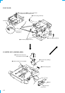
Flexible Circuit Board Repairing
• Keep the temperature of the soldering iron around 270 ˚C dur-
ing repairing.
• Do not touch the soldering iron on the same conductor of the
circuit board (within 3 times).
• Be careful not to apply force on the conductor when soldering
or unsoldering.
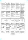
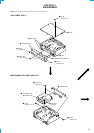
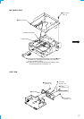
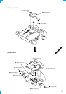
NOTES ON HANDLING THE OPTICAL PICK-UP
BLOCK OR BASE UNIT
SAFETY-RELATED COMPONENT WARNING!!
COMPONENTS IDENTIFIED BY MARK 0 OR DOTTED
LINE WITH MARK 0 ON THE SCHEMATIC DIAGRAMS
AND IN THE PARTS LIST ARE CRITICAL TO SAFE
OPERATION. REPLACE THESE COMPONENTS WITH
SONY PARTS WHOSE PART NUMBERS APPEAR AS
SHOWN IN THIS MANUAL OR IN SUPPLEMENTS PUB-
LISHED BY SONY.
CAUTION
Use of controls or adjustments or performance of procedures
other than those specified herein may result in hazardous ra-
diation exposure.
The laser diode in the optical pick-up block may suffer electro-
static break-down because of the potential difference generated
by the charged electrostatic load, etc. on clothing and the human
body.
During repair, pay attention to electrostatic break-down and also
use the procedure in the printed matter which is included in the
repair parts.
The flexible board is easily damaged and should be handled with
care.
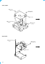
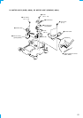
NOTES ON LASER DIODE EMISSION CHECK
Never look into the laser diode emission from right avove when
checking it for adustment. It is feared that you will lose your sight.
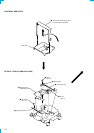
NOTES ON HANDLING THE OPTICAL PICK-UP BLOCK
(KMS-241C/J1NP).
The laser diode in the optical pick-up block may suffer electro-
static break-down easily. When handling it, perform soldering
bridge to the laser-tap on the flexible board. Also perform m easures
against electrostatic break-down sufficiently before the operation.
The flexible board is easily damaged and should be handled with
care.
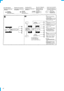
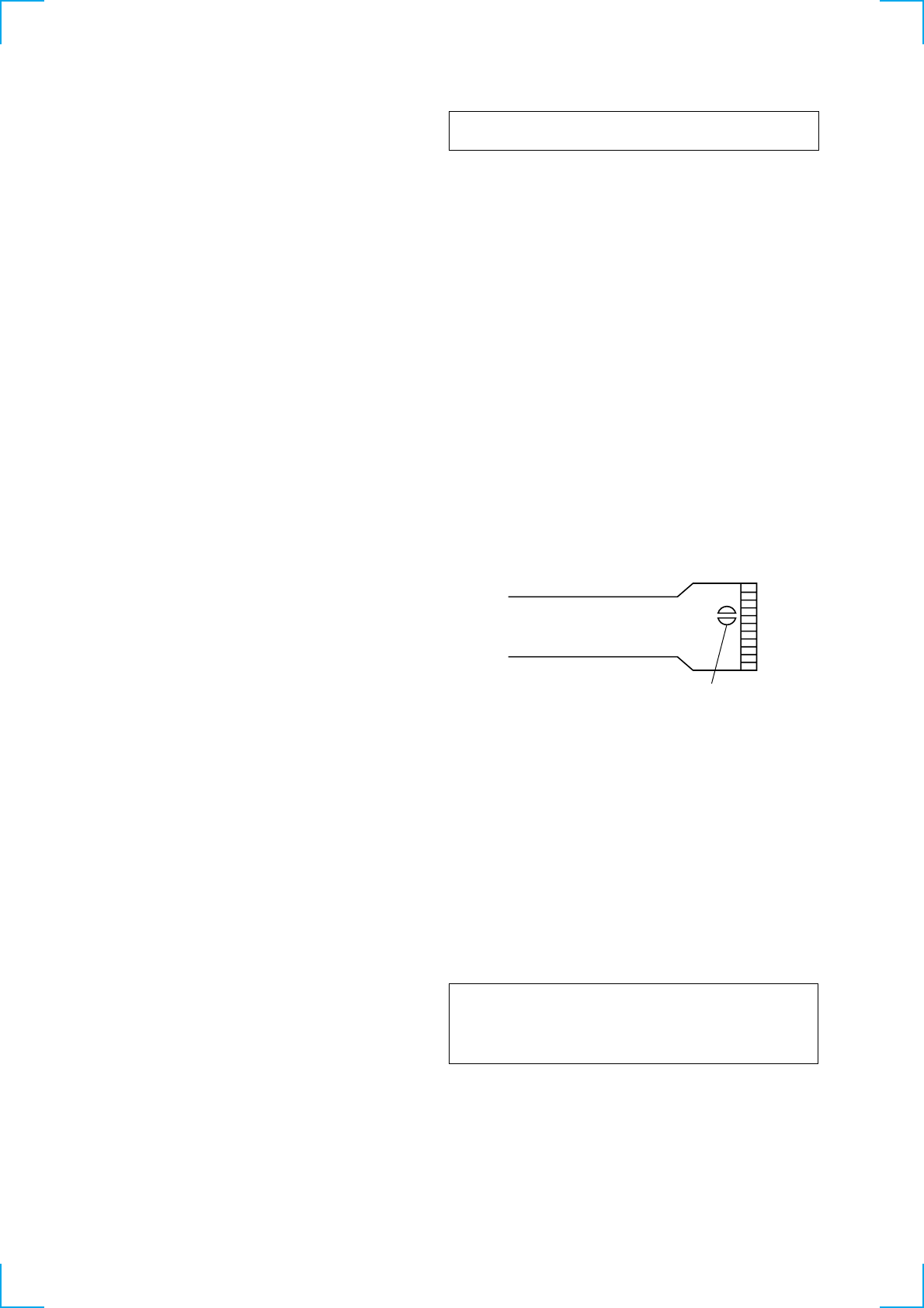
laser-tap
OPTICAL PICK-UP FLEXIBLE BOARD
1. GENERAL
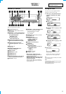
Location of controls ........................................................ 3
Installation ....................................................................... 4
Connections ..................................................................... 5
2. DISASSEMBLY ......................................................... 9
3. ELECTRICAL ADJUSTMENTS
Test Mode ........................................................................ 16
MD Section ..................................................................... 16
Tuner Section .................................................................. 16
4. DIAGRAMS
4-1. Block Diagram – SERVO Section – ............................... 17
4-2. Block Diagram – TUNER Section – .............................. 18
4-3. Block Diagram – MAIN Section – ................................. 19
4-4. Block Diagram – BUS CONTROL/
POWER SUPPLY Section – ........................................... 20
4-5. Note for Printed Wiring Boards and
Schematic Diagrams ....................................................... 21
4-6. Printed Wiring Boards
– SERVO Board (Component Side)/
SENSOR Board –............................................................ 22
4-7. Printed Wiring Board
– SERVO Board (Conductor Side) – .............................. 23
4-8. Schematic Diagram – SERVO Board (1/2) – ................. 24
4-9. Schematic Diagram – SERVO Board (2/2) – ................. 25
4-10. Printed Wiring Board
– MAIN Board (Component Side) – .............................. 26
4-11. Printed Wiring Board
– MAIN Board (Conductor Side) – ................................ 27
4-12. Schematic Diagram – MAIN Board (1/3) – ................... 28
4-13. Schematic Diagram – MAIN Board (2/3) – ................... 29
4-14. Schematic Diagram – MAIN Board (3/3) – ................... 30
4-15. Printed Wiring Board – SUB Board – ............................ 32
4-16. Schematic Diagram – SUB Board – ............................... 33
4-17. Printed Wiring Board – KEY Board – ............................ 34
4-18. Schematic Diagram – KEY Board – .............................. 35
4-19. IC Pin Function Description ........................................... 40
5. EXPLODED VIEWS ................................................ 50
6. ELECTRICAL PARTS LIST ............................... 54
TABLE OF CONTENTS