


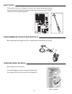
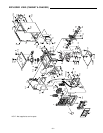
- 13 -
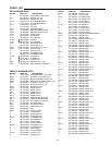
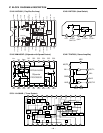
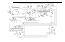
IC102 LC78622NE (Digital Signal Processor)
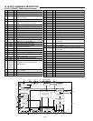
No. Pin Name I/O Function
32 TEST3 I Test pin.
33 TEST4 I Test pin.
34 NC - Non connection.
35 MUTEL O Mute output terminal for L-ch
36 LVDD - Power supply for L-ch
37 LCHO O Output terminal for L-ch
38 LVSS - GND for L-ch
39 RVSS - GND for R-ch
40 RCHO O Output terminal for R-ch
41 RVDD - Power supply for R-ch
42 MUTER O Mute output terminal for R-ch
43 XVDD - Power supply of crystal oscillation
44 XOUT O Connection terminal of crystal oscillation (16.9344MHz)
45 XIN I Connection terminal of crystal oscillation (16.9344MHz)
46 XVSS - GND of crystal oscillation
47 SBSY O Output terminal for synchronizing signal of
sub-cord block
48 EFLG O Output terminal for correction monitor of C1, C2,
Single and Double
49 PW O Output terminal for sub-cord of P, Q, R, S, T, U and W
50 SFSY O Output terminal for synchronizing signal of
sub-cord frame
51 SBCK I Input terminal for readout clock of sub-cord
52 FSX O Output terminal of Synchronizing signal (7.35kHz)
53 WRQ O Output terminal for standby of sub-cord Q output
54 RWC I Input terminal of read / write control
55 SQOUT O Output terminal of sub-cord Q
56 COIN I Input terminal of command from micro processor
57 CQCK I Clock input for reading sub-cord from SQOUT
58 RES I Reset (turn on : L)
59 TST11 O Test pin
60 16M O 16.9344MHz
61 4.2M O 4.2336MHz
62 TEST5 I Test pin
63 CS I Chip select terminal
64 TEST1 I Test pin
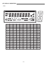
EFMO VV
DD
VV
SS
PDO ISET FR PCK TAI
TST11
TEST1 TEST3 TEST5
TEST2 TEST4
V
DD
V
SS
C2F
DOUT
(NC)
LV
DD
LV
SS
MUTELLCHO
MUTER
RV
DD
RV
SS
RCHO
XV
DD
XOUT
XINFSX
XV
SS
4.2M16MEFLGEMPHCONT5
CONT4
CONT3
CONT2
CONT1
TGL
RESJP+JP-TOFFTESHFL
RWC
COIN
CQCK
SQOUT
WRQ
CS
SFSY
SBSY
SBCK
PW
V/P
CLV-
CLV+
FSEQ
EFMIN
DEFI
10
22
1
12
13
14
49
51
47
50
63
53
55
57
56
54
15 16 17 20 19 58 18 24 25 26 27 28 29 48 60 61 46 52 45 44 43 39 41 42 40 37 35 38 36
34
31
30
9
21
6
4
357 2
59 64 11 32 33 62
8
23
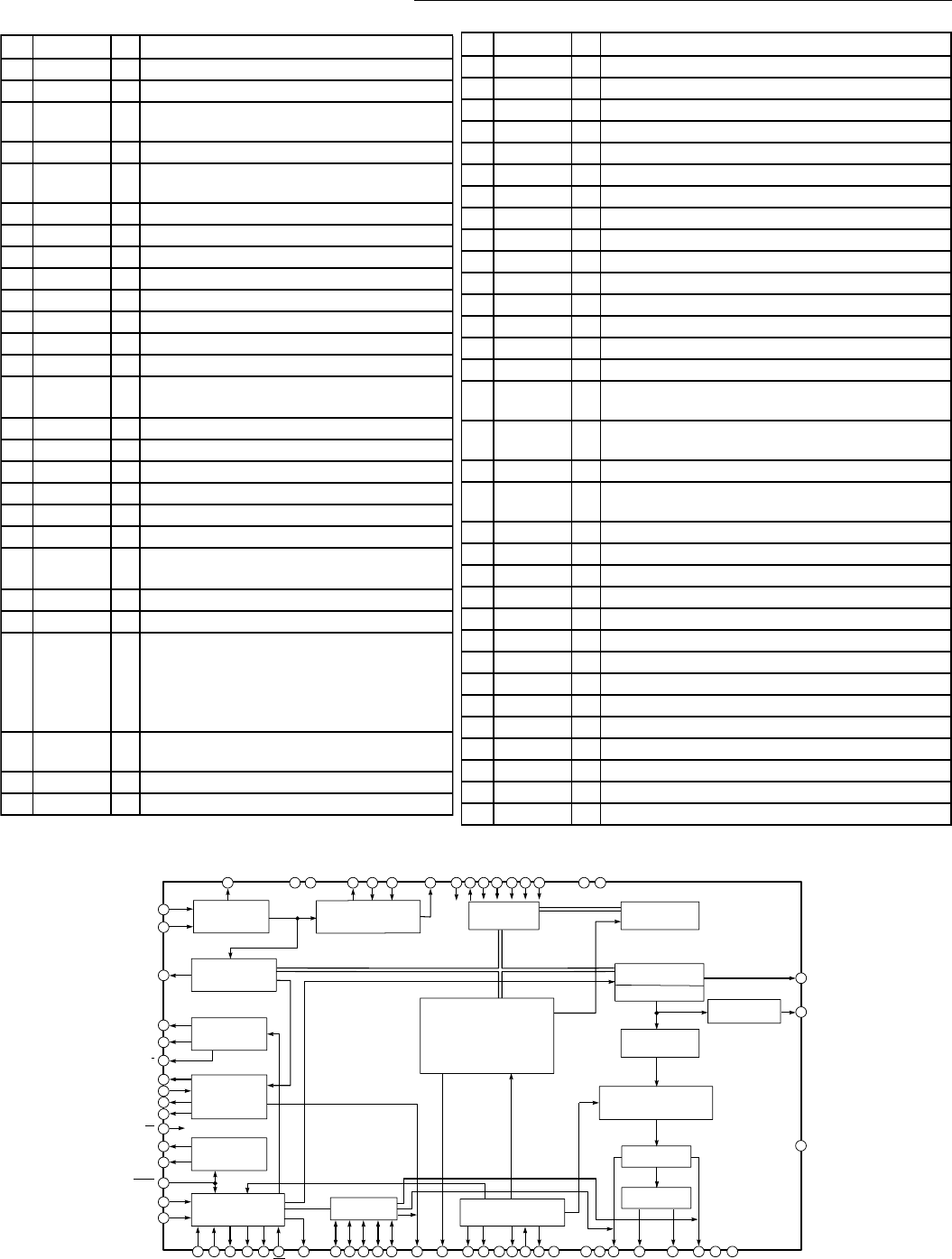
Slice level
Control
Subcode Dxract
QCRC
Syncrnous Detect
EFM Demodulation
VCO Clock Oscillator
& Clock Control
X'tal Root
Timing Generator
RAM Address
Generatorl
2KA~8bit
RAM
Billingual
Digital Out
General Ports
Digital Attenuator
Quadruple Over Sampling
Digital Filter
Interpolalation Mute
C1 C2 Error Detect &
Correct Control Flag
1bit DAC
L.P.F
CLV
Digital Servo
µCOM
Inter Fase
Servo Commander
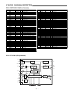
No. Pin Name I/O Function
1 DEFI I Input terminal for detect signal of defect
2 TAI I Input terminal for test.
3 PDO O The phase comparison output terminal for
external VCO control.
4 VVSS - Ground terminal for built-in VCO
5 ISET I Resistance connection terminal for
electric current adjustment of PDO output.
6 VVDD - Built-in VCO power supply terminal.
7 FR I VCO frequency range adjustment.
8 VSS - Ground for Digital
9 EFMO O EFM signal output terminal for slice level control.
10 EFMIN I EFM signal input terminal for slice level control.
11 TEST2 I TEST pin. Normal time is non connection.
12 CLV+ O Output terminal for Disc motor control.
13 CLV- O Output terminal for Disc motor control.
14 V/P O Change of rough servo / phase control
Rough servo : "H", Phase control : "L"
15 HFL I Input terminal of track search signal.
16 TES I Input terminal of tracking error signal.
17 TOFF O Output terminal of tracking off.
18 TGL O Output terminal for change of tracking gain.
19 JP+ O Output terminal for tracking jump control.
20 JP- O Output terminal for tracking jump control.
21 PCK O Clock monitor output terminal for EFM data
playback. (4.3218 MHz)
22 FSEQ O Output terminal for detect of SYNC signal.
23 DVDD - +5V
24 CONT1 I/O
25 CONT2 I/O This output can control at serial control from
26 CONT3 I/O micro processor.
27 CONT4 I/O
28 CONT5 I/O
29 EMPH O Output terminal of de-emphasis monitor .
"H" : de-emphasis
30 C2F O Output terminal of C2 flag
31 DOUT O Output terminal of digital out
IC BLOCK DIAGRAM & DESCRIPTION