


HA17458 Series
Rev.1.00 Jun 15, 2005 page 3 of 8
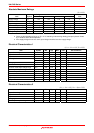
Absolute Maximum Ratings
(Ta = 25°C)
Ratings
Item Symbol
HA17458 HA17458PS HA17458F HA17458FP
Unit
Supply voltage V
CC
+18 +18 +18 +18 V
V
EE
–18 –18 –18 –18 V
Intput voltage V
IN
*
3
±15 ±15 ±15 ±15 V
Differential input voltage V
IN(diff)
±30 ±30 ±30 ±30 V
Power dissipation P
T
670*
1
670*
1
385*
2
385*
2
mW
Operating temperature Topr –20 to +75 –20 to +75 –20 to +75 –20 to +75 °C
Storage temperature Tstg –55 to +125 –55 to +125 –55 to +125 –55 to +125 °C
Notes: 1. These are the allowable values up to Ta = 45 °C. Derate by 8.3mW/°C above that temperature.
2. These are the allowable values up to Ta = 31 °C mounting on 30% wiring density glass epoxy board. Derate
by 7.14mW/°C above that temperature.
3. If the supply voltage is less than ±15V, input voltage should be less than supply voltage.
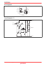
Electrical Characteristics 1
(V
CC
= –V
EE
= 15V, Ta = 25°C)
Item Symbol Min Typ Max Unit Test conditions
Input offset voltage V
IO
— 2.0 6.0 mV R
S
≤ 10kΩ
Input offset current I
IO
— 6 200 nA
Input bias current I
IB
— 30 500 nA
Line regulation ∆V
IO
/∆V
CC
— 30 150 µV/V R
S
≤ 10kΩ
∆V
IO
/∆V
EE
— 30 150 µV/V R
S
≤ 10kΩ
Voltage gain A
VD
86 100 — dB R
L
≥ 2kΩ, Vout = ±10V
Common mode rejection ratio CMR 70 90 — dB R
S
≤ 10kΩ
Common mode input voltage range V
CM
±12 ±13 — V
Peak-to-peak output voltage Vop-p ±12 ±14 — V R
L
= 10kΩ
Power dissipation P
d
— 90 200 mW No load, 2 channel
Slew rate SR — 0.6 — V/µs A
VD
= 1
Input resistance Rin 0.3 1.0 — MΩ
Input capacitance Cin — 6.0 — pF
Output resistance Rout — 75 — Ω
Electrical Characteristics 2
(V
CC
= –V
EE
= 15V, Ta = –20 to +75°C)
Item Symbol Min Typ Max Unit Test conditions
Input offset voltage V
IO
— — 9.0 mV R
S
≤ 10kΩ
Input offset current I
IO
— — 400 nA
Input bias current I
IB
— — 1100 nA
Voltage gain A
VD
80 — — dB R
L
≥ 2kΩ, Vout = ±10V
Peak-to-peak output voltage Vop-p ±10 ±13 — V R
L
= 2kΩ