


3SK318
Rev.2.00 Aug 10, 2005 page 3 of 7
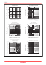
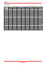
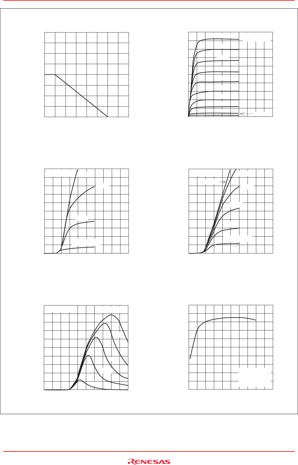
200
150
100
50
0
50 100 150
200
Channel Power Dissipation Pch (mW)
Ambient Temperature Ta (°C)
Maximum Channel Power
Dissipation Curve
0
2468
10
V
G2S
= 3 V
Drain to Source Voltage V
DS
(V)
Drain Current I
D
(mA)
Typical Output Characteristics
4
8
12
16
20
0.9 V
1.0 V
1.1 V
1.2 V
1.3 V
1.6 V
1.5 V
1.4 V
V
G1S
= 1.7 V
0.8 V
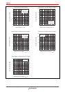
20
16
12
8
4
0
12 345
Drain Current I
D
(mA)
Gate1 to Source Voltage V
G1S
(V)
Drain Current vs.
Gate1 to Source Voltage
V
DS
= 3.5 V
2.0 V
2.5 V
1.5 V
V
G2S
= 1.0 V
20
16
12
8
4
0
12345
Drain Current I
D
(mA)
Gate2 to Source Voltage V
G2S
(V)
Drain Current vs.
Gate2 to Source Voltage
V
DS
= 3.5 V
V
G1S
= 1.0 V
1.2 V
1.4 V
1.6 V
1.8 V
2.0 V
25
20
15
10
5
0
5101520
25
30
24
18
12
6
0
0.4 0.8 1.2 1.6 2.0
V
G2S
= 3 V
1 V
2 V
Forward Transfer Admittance |y
fS
| (mS)
Gate1 to Source Voltage V
G1S
(V)
Power Gain PG (dB)
Drain Current I
D
(mA)
Power Gain vs. Drain Current
Forward Transfer Admittance
vs. Gate1 Voltage
V
DS
= 3.5 V
1.5 V
2.5 V
V
DS
= 3.5 V
V
G2S
= 3 V
f = 900 MHz