


July 1994 6
Philips Semiconductors Product specification
1 W BTL mono audio amplifier with DC
volume control
TDA7052A/AT
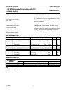
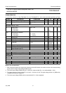
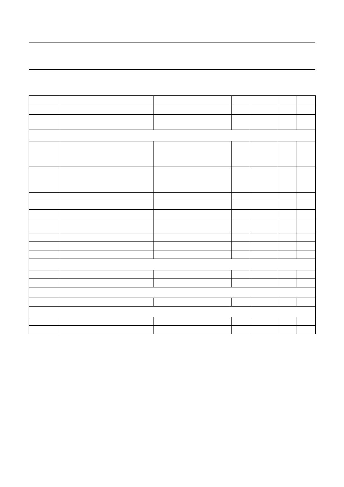
CHARACTERISTICS
V
P
= 6 V; T
amb
= 25 °C; f = 1 kHz; TDA7052A: R
L
= 8 Ω; TDA7052AT: R
L
= 16 Ω; unless otherwise specified (see Fig.6).
Notes to the characteristics
1. With a load connected to the outputs the quiescent current will increase, the maximum value of this increase being
equal to the DC output offset voltage dividend by R
L
.
2. The noise output voltage (RMS value) at f = 500 kHz is measured with R
S
= 0 Ω and bandwidth = 5 kHz.
3. The ripple rejection is measured with R
S
= 0 Ω and f = 100 Hz to 10 kHz. The ripple voltage of 200 mV, (RMS value)
is applied to the positive supply rail.
4. The noise output voltage (RMS value) is measured with R
S
= 5 kΩ unweighted.
SYMBOL PARAMETER CONDITIONS MIN. TYP. MAX. UNIT
V
P
positive supply voltage range 4.5 − 18 V
I
P
total quiescent current V
P
= 6 V; R
L
= ∞
note 1
− 712mA
Maximum gain; V
4
= 1.4 V
P
O
output power THD = 10%
TDA7052A 1.0 1.1 − W
TDA7052AT 0.5 0.55 − W
THD total harmonic distortion
TDA7052A P
O
= 0.5 W − 0.3 1 %
TDA7052AT P
O
= 0.25 W − 0.3 1 %
G
v
voltage gain 34.5 35.5 36.5 dB
V
I
input signal handling V
4
= 0.8 V; THD < 1% 0.5 0.65 − V
V
no(rms)
noise output voltage (RMS value) f = 500 kHz; note 2 − 210 −µV
B bandwidth −1 dB − 20 Hz to
300 kHz
−
SVRR supply voltage ripple rejection note 3 38 46 − dB
|V
off
| DC output offset voltage − 0 150 mV
Z
I
input impedance (pin 2) 15 20 25 kΩ
Minimum gain; V
4
= 0.5 V
G
v
voltage gain −−44 − dB
V
no(rms)
noise output voltage (RMS value) note 4 − 20 30 µV
Mute position
V
O
output voltage in mute position V
4
≤ 0.3 V; V
I
= 600 mV −− 30 µV
DC volume control
φ gain control range 75 80 − dB
I
4
control current V
4
= 0.4 V 60 70 80 µA