


June 1989 4
Philips Semiconductors Product specification
Low voltage mono/stereo power amplifier TDA7050
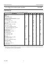
CHARACTERISTICS
V
P
= 3 V; f = 1 kHz; R
L
= 32 Ω; T
amb
= 25 °C; unless otherwise specified
Note
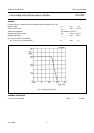
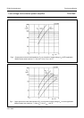
1. Output power is measured directly at the output pins of the IC. It is shown as a function of the supply voltage in Fig.2
(BTL application) and Fig.3 (stereo application).
PARAMETER SYMBOL MIN. TYP. MAX. UNIT
Supply
Supply voltage V
P
1,6 − 6,0 V
Total quiescent current I
tot
− 3,2 4 mA
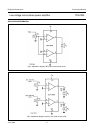
Bridge-tied load application (BTL); see Fig.4
Output power; note 1
V
P
= 3,0 V; d
tot
= 10% P
o
− 140 − mW
V
P
= 4,5 V; d
tot
= 10% (R
L
= 64 Ω)P
o
−150 − mW
Voltage gain G
v
− 32 − dB
Noise output voltage (r.m.s. value)
R
S
= 5 kΩ; f = 1 kHz V
no(rms)
− 140 −µV
R
S
= 0 Ω; f = 500 kHz; B = 5 kHz V
no(rms)
− tbf −µV
D.C. output offset voltage (at R
S
= 5 kΩ)|∆V| −−70 mV
Input impedance (at R
S
= ∞)|Z
i
|1 −−MΩ
Input bias current I
i
− 40 − nA
Stereo application; see Fig.5
Output power; note 1
V
P
= 3,0 V; d
tot
= 10% P
o
− 35 − mW
V
P
= 4,5 V; d
tot
= 10% P
o
− 75 − mW
Voltage gain G
v
24.5 26 27.5 dB
Noise output voltage (r.m.s. value)
R
S
= 5 kΩ; f = 1 kHz V
no(rms)
− 100 −µV
R
S
= 0 Ω; f = 500 kHz; B = 5 kHz V
no(rms)
− tbf −µV
Channel separation
R
S
= 0 Ω; f = 1 kHz α 30 40 − dB
Input impedance (at R
S
= ∞)|Z
i
|2 −−MΩ
Input bias current I
i
− 20 − nA