


1997 Aug 14 5
Philips Semiconductors Preliminary specification
2 × 23 W high efficiency car radio power
amplifier
TDA1561Q
FUNCTIONAL DESCRIPTION
The TDA1561Q contains two identical amplifiers with
differential inputs. At low output power (up to output
amplitudes of 3 V (RMS) at V
P
= 14.4 V), the device
operates as a normal SE amplifier. When a larger output
voltage swing is needed, the circuit switches internally to
BTL operation.
With a sine wave input signal the dissipation of a
conventional BTL amplifier up to 2 W output power is more
than twice the dissipation of the TDA1561Q (see Fig.9).
In normal use, when the amplifier is driven with music-like
signals, the high (BTL) output power is only needed for a
small percentage of time. Under the assumption that a
music signal has a normal (Gaussian) amplitude
distribution, the dissipation of a conventional BTL amplifier
with the same output power is approximately 70% higher
(see Fig.10).
The heatsink has to be designed for use with music
signals. With such a heatsink, the thermal protection will
disable the BTL mode when the junction temperature
exceeds 145 °C. In this case the output power is limited to
5 W per amplifier.
The gain of each amplifier is internally fixed at 32 dB. With
the MODE pin, the device can be switched to the following
modes:
• Standby with low standby current (<50 µA)
• Mute condition, DC adjusted
• On, operation
• SE-only, operation (BTL disabled).
The device is fully protected against short-circuiting of the
output pins to ground and to the supply voltage. It is also
protected against short-circuiting the loudspeaker and
high junction temperatures. In the event of a permanent
short-circuit condition to ground or the supply voltage, the
output stage will be switched off causing a low dissipation.
With permanent short-circuiting of the loudspeaker, the
output stage will be repeatedly switched on and off.
The duty cycle in the ‘on’ condition is low enough to
prevent excessive dissipation.
To avoid plops during switching from ‘mute’ to ‘on’ or from
‘on’ to ‘mute/standby’ while an input signal is present, a
built-in zero-crossing detector allows only switching at
zero input voltage. However, when the supply voltage
drops below 6 V (e.g. engine start), the circuit mutes
immediately avoiding clicks coming from electronic
circuitry preceding the power amplifier.
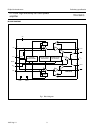
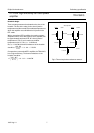
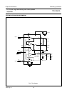
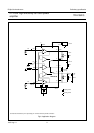
The voltage of the SE electrolytic capacitor (pin 11) is
always kept at 0.5V
P
by means of a voltage buffer (see
Fig.1). The value of this capacitor has an important
influence on the output power in SE mode, especially at
low signal frequencies, a high value is recommended to
minimize dissipation at low frequencies.