


2003 Sep 18 5
Philips Semiconductors Product specification
MMIC wideband medium power amplifier BGA6489
APPLICATION INFORMATION
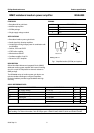
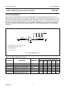
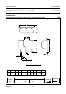
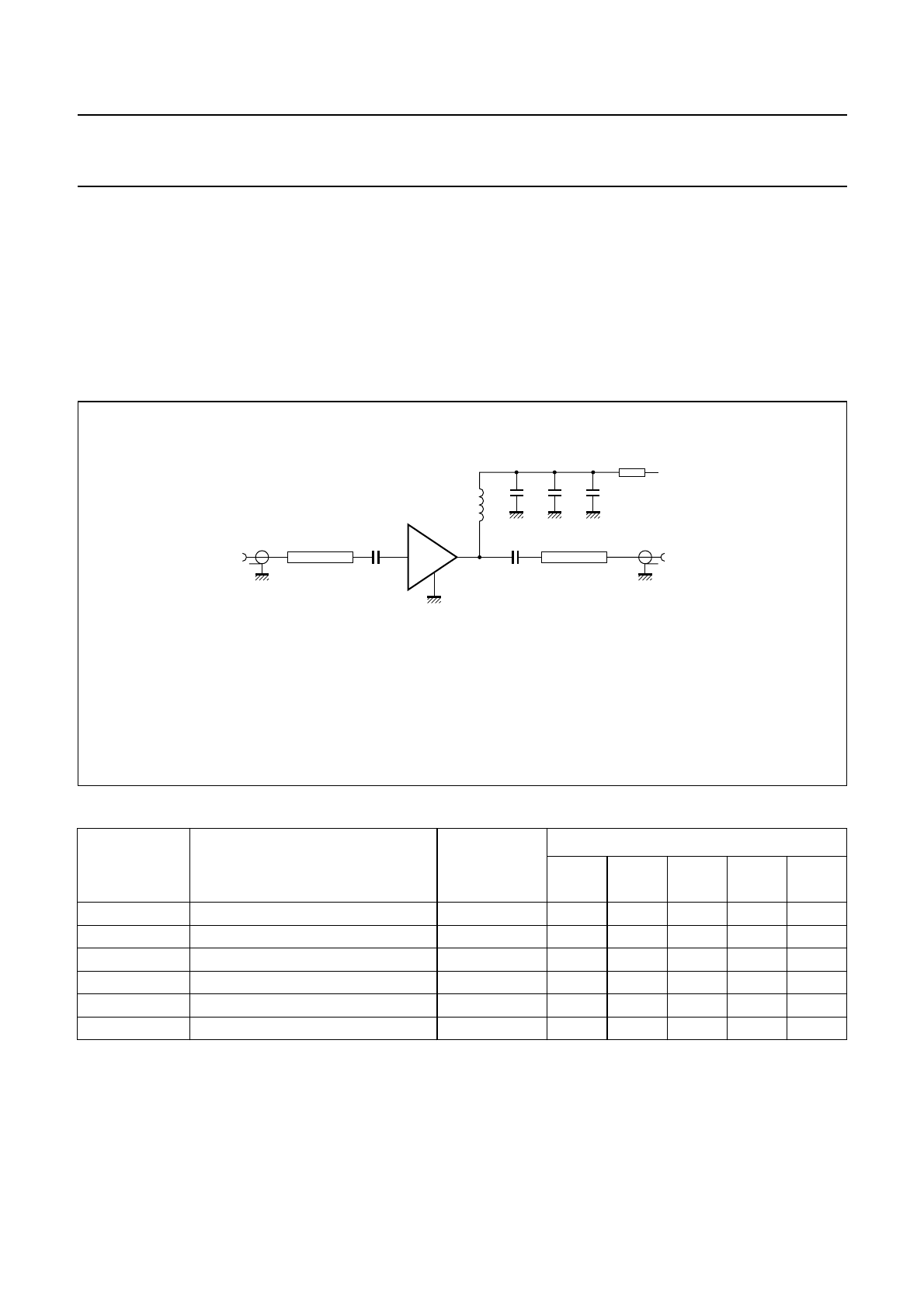
Figure 2 shows a typical application circuit for the BGA6489 MMIC. The device is internally matched to 50 Ω, and
therefore does not require any external matching. The value of the input and output DC blocking capacitors C1 and C2
depends on the operating frequency; see the tables below. Capacitors C1 and C2 are used in conjunction with L1 and
C3 to fine tune the input and output impedance. For optimum supply decoupling, a 1 µF capacitor (C5) can be added.
The external components should be placed as close as possible to the MMIC. When using via holes, use multiple via
holes per pin in order to limit ground path induction. Resistor R1 is a bias resistor providing DC current stability with
temperature.
handbook, full pagewidth
50 Ω
microstrip
C1 C2
C3
L1
V
D
V
S
50 Ω
microstrip
C4 C5
(1)
R1
(2)
MGX419
1
2
3
Fig.2 Typical application circuit.
(1) Optional capacitor for optimum supply decoupling.
(2) R1 values at operating supply voltage:
V
S
= 6 V; R1 = 15 Ω.
V
S
= 9 V; R1 = 51 Ω.
V
S
= 11.5 V; R1 = 82 Ω.
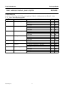
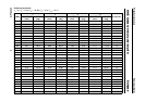
Table 1 Component descriptions (see Fig.2)
COMPONENT DESCRIPTION DIMENSIONS
VALUE AT OPERATING FREQUENCY
500
MHz
800
MHz
1950
MHz
2400
MHz
3500
MHz
C1, C2 multilayer ceramic chip capacitor 0603 220 pF 100 pF 68 pF 56 pF 39 pF
C3 multilayer ceramic chip capacitor 0603 1 nF 1 nF 1 nF 1 nF 1 nF
C4 multilayer ceramic chip capacitor 0603 100 pF 68 pF 22 pF 22 pF 15 pF
C5 (optional) electrolytic or tantalum capacitor 0603 1 µF1µF1µF1µF1µF
L1 SMD inductor 0603 68 nH 33 nH 22 nH 18 nH 15 nH
R1 SMD resistor 0.5 W; V
S
=9V − −−−−−