


CGD942C_1 © NXP B.V. 2007. All rights reserved.
Product data sheet Rev. 01 — 7 June 2007 2 of 7
NXP Semiconductors
CGD942C
870 MHz, 23 dB gain power doubler amplifier
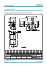
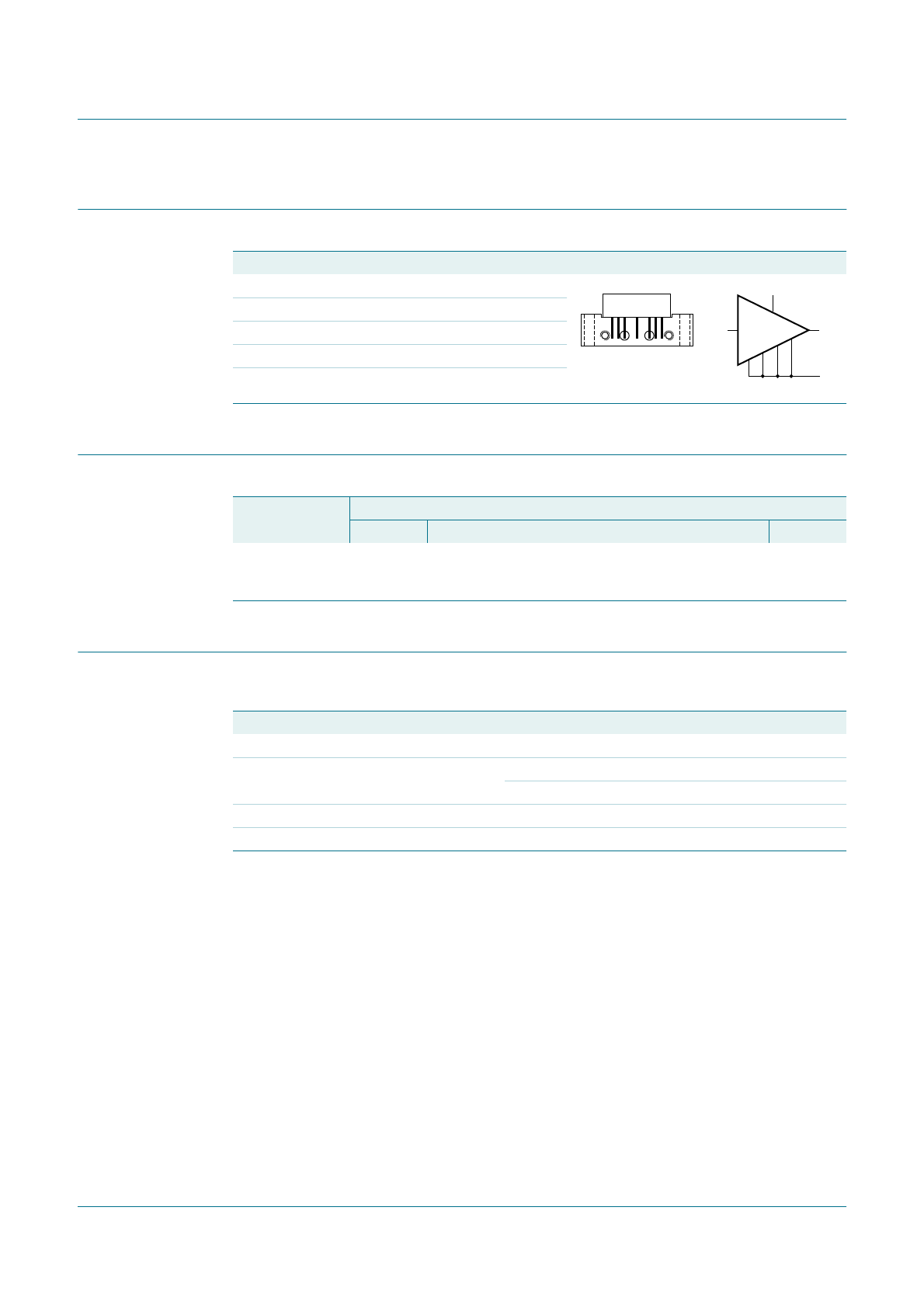
2. Pinning information
3. Ordering information
4. Limiting values
Table 2. Pinning
Pin Description Simplified outline Symbol
1 input
2, 3 common
5+V
B
7, 8 common
9 output
91357
2378
5
91
sym095
Table 3. Ordering information
Type number Package
Name Description Version
CGD942C - rectangular single-ended package; aluminium flange;
2 vertical mounting holes; 2 × 6-32 UNC and 2 extra
horizontal mounting holes; 7 gold-plated in-line leads
SOT115J
Table 4. Limiting values
In accordance with the Absolute Maximum Rating System (IEC 60134).
Symbol Parameter Conditions Min Max Unit
V
B
supply voltage - 30 V
V
i(RF)
RF input voltage single tone - 75 dBmV
132 channels flat - 45 dBmV
T
stg
storage temperature −40 +100 °C
T
mb
mounting base temperature −20 +100 °C