


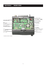
SECTION 4 CIRCUIT DESCRIPTION
4 - 1
4-1 RECEIVER CIRCUITS
4-1-1 ANTENNA SWITCHING CIRCUIT
(MAIN UNIT)
The antenna switching circuit functions as a low-pass filter
while receiving and as resonator circuit while transmitting.
This circuit does not allow transmit signals to enter the
receiver circuits.
Received signals enter the antenna connector and pass
through the low-pass filter (L1–L3, C1, C2, C6–C8). The fil-
tered signals are then applied to the RF circuit passed
through the λ⁄4 type antenna switching circuit (D5, D6, D41,
L6).
4-1-2 RF CIRCUIT (MAIN UNIT)
The RF circuit amplifies signals within the range of frequen-
cy coverage and filters out-of-band signals.
The signals from the antenna switching circuit pass through
the two-stage tunable bandpass filters (D8, D4). The filtered
signals are amplified at the RF amplifier (Q2) and then enter
other two-stage bandpass filters (D9, D10) to suppress
unwanted signals. The filtered signals are applied to the 1st
mixer circuit (Q3).
The tunable bandpass filters (D4, D8–D10) employ varactor
diodes to tune the center frequency of the RF passband for
wide bandwidth receiving and good image response rejec-
tion. These diodes are controlled by the CPU (FRONT unit;
IC1) via the D/A converter (IC6).
The gate control circuit reduces RF amplifier gain and atten-
uates RF signal to keep the audio output at a constant level.
The receiver gain is determined by the voltage on the “RSSI”
line from the FM IF IC (IC1, pin 12). The gate control circuit
(Q1) supplies control voltage to the RF amplifier (Q2) and
sets the receiver gain.
When receiving strong signals, the “RSSI” voltage increases
and the gate control voltage decreases. As the gate control
voltage is used for the bias voltage of the RF amplifier (Q2),
then the RF amplifier gain is decreased.
4-1-3 1ST MIXER AND 1ST IF CIRCUITS
(MAIN UNIT)
The 1st mixer circuit converts the received signals to a fixed
frequency of the 1st IF signal with the PLL output frequency.
By changing the PLL frequency, only the desired frequency
will pass through a MCF (Monolithic Crystal Filter; FI1) at the
next stage of the 1st mixer.
The RF signals from the bandpass filter are applied to the
1st mixer circuit (Q3). The applied signals are mixed with the
1st LO signal coming from the RX VCO circuit (Q14) to pro-
duce a 46.35 MHz 1st IF signal. The 1st IF signal passes
through a MCF (Monolithic Crystal Filter; FI1) to suppress
out-of-band signals. The filtered signal is amplified at the 1st
IF amplifier (Q4) and applied to the 2nd IF circuit.
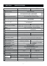
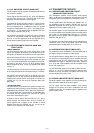
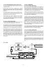
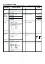
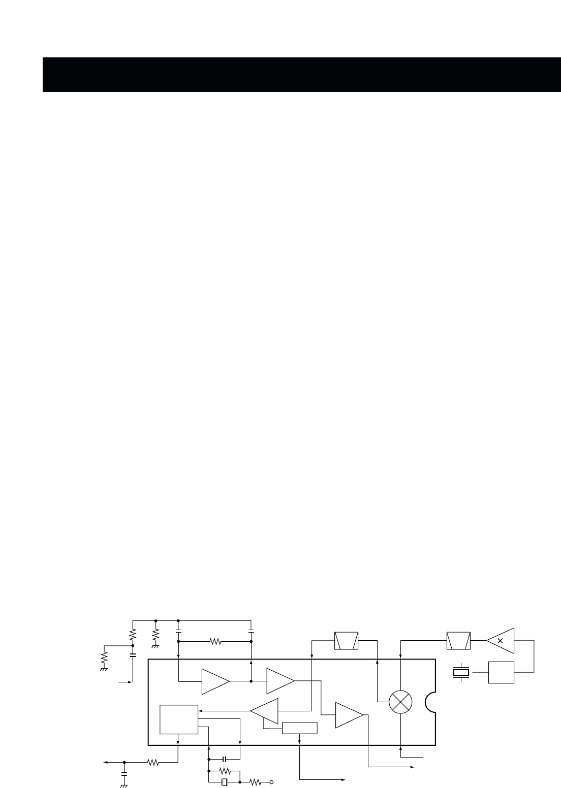
4-1-4 2ND IF AND DEMODULATOR CIRCUITS
(MAIN UNIT)
The 2nd mixer circuit converts the 1st IF signal to a 2nd IF
signal. A double-conversion superheterodyne system
improves the image rejection ratio and obtains stable receiv-
er gain.
The 1st IF signal from the 1st IF amplifier (Q4) is applied to
the 2nd mixer section of the FM IF IC (IC1, pin 16) and is
then mixed with the 2nd LO signal for conversion to a 450
kHz 2nd IF signal.
IC1 contains the 2nd mixer, limiter amplifier, quadrature
detector, active filter and noise amplifier circuits, etc. A
tripled frequency from the PLL reference oscillator is used
for the 2nd LO signal (45.9 MHz).
The 2nd IF signal from the 2nd mixer (IC1, pin 3) passes
through a ceramic filter (FI2) to remove unwanted hetero-
dyned frequencies. It is then amplified at the limiter amplifi-
er section (IC1, pin 5) and applied to the quadrature detec-
tor section (IC1, pins 10, 11 and X1) to demodulate the 2nd
IF signal into AF signals.
The AF signals are output from pin 9 (IC1) and are then
applied to the AF amplifier circuit.
• 2nd IF and demodulator circuits
FI2
2nd IF filter
450 kHz
Q34
IC4
Limiter
amp.
Noise
amp.
Noise
comp.
FM
detector
Active
filter
AF signals
5V
X1
RSSI
2nd
Mixer
X2
15.3 MHz
45.9 MHz
1st IF from the IF amplifier (Q4)
"NOIS" signal to the CPU
"RSSI" signal to the CPU
8
7
5
BPF
PLL
IC
32
3
16131211109
IC1
TA31136FN
"SQLIN" signal
from the D/A
converter IC (IC6).
("DET" signal)