


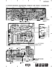
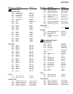
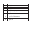

37
VSX-D307
No. Pin Name I/O Function
33 XTLI I Crystal oscillation circuit input
34 AVSX – Analog ground for master clock
35 XSOUT O S-ch D/A converter output
36 AVS6 – Ground for S-ch D/A converter
37 AVD6 – Power supply for S-ch D/A converter
38 RIN I Analog input of R-ch A/D converter
39 LO2 O OP amp. inverting output for LPF of R-ch A/D converter
40 AVS2 – Ground for R-ch A/D converter
41 AVD2 – Power supply for R-ch A/D converter
42 ROUT O R-ch D/A converter output
43 AVD4 – Power supply for R-ch D/A converter
44 AVS4 – Ground for R-ch D/A converter
45 VSS3 – Digital ground
46 SCK I Shift clock input of microprocessor interface
47 REDY O Transfer permission signal output of microprocessor interface L : Transfer prohibition
48 T.P – Monitor pin for test Normally, outputs "Hi-Z".
49 XLAT I Latch input of microprocessor interface
50 RVDT I Data input of microprocessor interface
51 XS24 I 24/32 bit slot selection of serial data L : 24 bit slot (It is effective at slave mode.)
52 VDD1 – Digital power supply
53 VSS4 – Digital ground
54 T.P – Monitor pin for test Normally, outputs "L".
55 SI I Serial data input of 1 sampling 2 channel
56 T.P – Input pin for test Normelly, outputs "L".
57 BCK I/O Serial bit transfer clock of serial input/output data SI and SO
58 LRCK I/O Sampling frequency clock of serial input/output data SI and SO
59 VSS5 – Digital ground
60 XMST I Master/slave mode switching input of BCK and LRCK L : master mode
61-63 T.P O Monitor pin for test Normally, outputs "L".
64 VSS6 – Digital ground
65-72 T.P O Monitor pin for test Normally, outputs "L".
73 VDD2 – Digital power supply
74 VSS7 – Digital ground
75-80 T.P O Monitor pin for test Normally, outputs "L".