


36
VSX-D307
No. Pin Name I/O Function
1-3 T.P O Monitor pin for test Normally, outputs "L".
4 VSS0 – Digital ground
5-8 T.P O Monitor pin for test Normally, outputs "L".
9 TST0 I Test pin Normally, fix to L.
10 VDD0 – Digital power supply
11 VSS1 – Digital ground
12 TST1 I Test pin Normally, fix to "L".
13 TST2 I Test pin Normally, fix to "L".
14 TST3 I Test pin Normally, fix to "L".
15 TST4 I Test pin Normally, fix to "L".
16 XRST I System reset input L : reset.
17 BFOT O Clock and divided frequency output (384/768/256/512 fs)
18 CSL1 I Test pin Normally, fix to "H".
19 CSL2 I Test pin Normally, fix to "L".
20 VSS2 – Digital ground
21 AVS3 – Ground for L-ch D/A converter
22 AVD3 – Power supply for L-ch D/A converter
23 LOUT O L-ch A/D converter output
24 AVD1 – Power supply for L-ch A/D converter
25 AVS1 – Ground for L-ch A/D converter
26 LO1 O OP amp. inverting output for LPF of L-ch A/D converter
27 LIN I Analog input of L-ch A/D converter
28 AVD5 – Power supply for C-ch D/A converter
29 AVS5 – Ground for C-ch D/A converter
30 XCOUT O C-ch D/A converter output
31 AVDX – Analog power supply for master clock
32 XTLO O Crystal oscillation circuit output
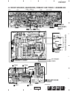
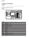
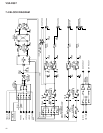
7. GENERAL INFORMATION
• The information shown in the list is basic information and may not correspond exactly to that shown in the schematic diagrams.
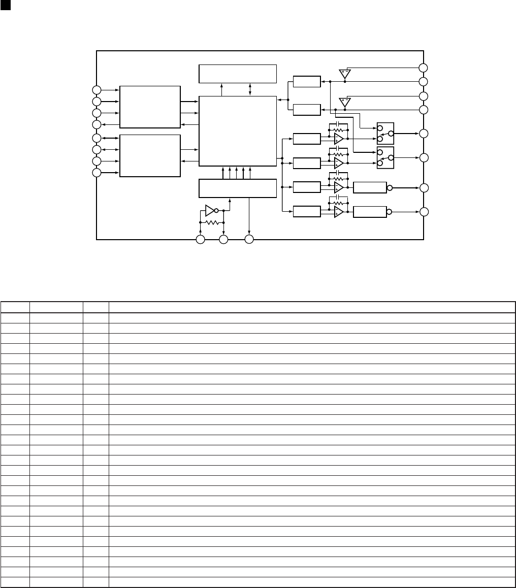
CXD2724Q (VOLUME DSP ASSY : IC201)
• DSP IC
•
Block Diagram
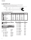
7.1 PARTS
7.1.1 IC
RVDT
SCK
XLAT
READY
LRCK
BCK
SI
XMST
50
46
49
47
58
57
55
60
XTLI
33
XTLO
32
BFOT
17
XSOUT
35
XCOUT
30
ROUT
42
LOUT
23
LO2
39
RIN
38
LO1
26
LIN
27
MICRO
COMPUTER
I/F
DSP
24k bit DELAY RAM
ADC1
ADC2
DAC1
DAC2
Trim Vol
Trim Vol
Analog SW
Analog SW
DAC3
DAC4
CLOCK GENERATOR
/TIMING CIRCUIT
SERIAL
DATA
I/F
•
Pin Function