Power Base-2 & 800CSL Amplifier Service Manual
9
Theory
tivity is achieved by controlling the ratio of feedback to
input resistance. The Sensitivity Switch sets the input
impedance to this stage and varies the gain such that
the overall amplifier gain is 26 dB, or is adjusted
appropriately for 0.775V or 1.4V input to attain rated
output. Note that earlier models (before main modules
built with D 7911-7 board) did not support the 1.4V
sensitivity.
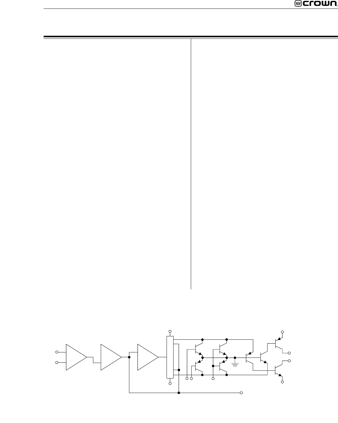
Error Amp
The inverted output from the VGS is fed to the non-
inverting input of the Error Amp op-amp stage through
an AC coupling capacitor and input resistor. Amplifier
output is fed back via the negative feedback (NFb)
loop resistor. The ratio of feedback resistor to input
resistor fixes gain from the Error Amp input to the
output of the amplifier at 26 dB. Diodes prevent
overdriving the Error Amp. Because the Error Amp
amplifies the difference between input and output
signals, any difference in the two waveforms will
produce a near open loop gain condition which in turn
results in high peak output voltage. The output of the
Error Amp, called the Error Signal (ES) drives the
Voltage Translators.
VOLTAGE AMPLIFICATION
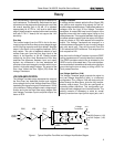
The Voltage Translator stage separates the output of
the Error Amp into balanced positive and negative
drive voltages for the Last Voltage Amplifiers (LVAs),
translating the signal from ground referenced ±15V to
±Vcc reference. LVAs provide the main voltage ampli-
fication and drive the High Side output stages. Gain
from Voltage Translator input to amplifier output is a
factor of 25.2.
Voltage Translators
A voltage divider network splits the Error Signal (ES)
into positive and negative drive signals for the bal-
anced voltage translator stage. These offset reference
voltages drive the input to the Voltage Translator
transistors. A nested NFb loop from the output of the
amplifier mixes with the inverted signal riding on the
offset references. This negative feedback fixes gain at
the offset reference points (and the output of the Error
Amp) at a factor of -25.2 with respect to the amplifier
output. The Voltage Translators are arranged in a
common base configuration for non-inverting voltage
gain with equal gain. They shift the audio from the
±15V reference to VCC reference. Their outputs drive
their respective LVA.
Also tied into the Voltage Translator inputs are ODEP
limiting transistors and control/protection transistors.
The ODEP transistors steal drive as dictated by the
ODEP circuitry (discussed later). The control/protec-
tion transistors act as switches to totally shunt audio to
ground during the turn-on delay, or during a DC/LF or
Fault protective action.
Last Voltage Amplifiers (LVAs)
The Voltage Translator stage channels the signal to
the Last Voltage Amplifiers (LVA's) in a balanced
configuration. The +LVA and -LVA, with their push-pull
effect through the Bias Servo, drive the fully comple-
mentary output stage. The LVAs are configured as
common emitter amplifiers. This configuration pro-
vides sufficient voltage gain and inverts the audio. The
polarity inversion is necessary to avoid an overall
polarity inversion from input jack to output jack, and it
+
-
+
-
+
-
BGS VGS Error
Amp
Audio
Inputs
Voltage Divider
NFb Loop
+
-
ODEP
Mute
+15V
-15V
+VCC
-VCC
NPN Outputs (+HS)
PNP Outputs (-HS)
Q100
Q103
Q121
Q122
Q101
Q102
Q105
Q110
Voltage
Translators
LVA's
Figure 1. Typical Amplifier Front End and Voltage Amplification Stages.


