Power Base-1 & 460CSL Amplifier Service Manual
12
Theory
±ODEP circuitry is used to simulate the thermal barri-
ers between the interior of the output device die
(immeasurable by normal means) and the time delay
from heat generation at the die until heat dissipates to
the thermal sensor. The combined effects of thermal
history and instantaneous dynamic power level result
in an accurate simulation of the actual thermal condi-
tion of the output transistors.
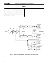
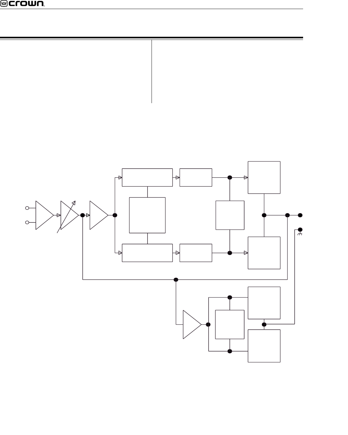
NEGATIVE
LOW SIDE
OUTPUT
PNP STAGE
POSITIVE
LOW SIDE
OUTPUT
NPN STAGE
NEGATIVE
HIGH SIDE
OUTPUT
PNP STAGE
POSITIVE
HIGH SIDE
OUTPUT
NPN STAGE
HIGH SIDE
BIAS
SERVO
+LVA
-1
-LVA
-1
+VOLTAGE
TRANSLATOR
-VOLTAGE
TRANSLATOR
OUTPUT
DEVICE
EMULATION
PROTECTION
ERROR
AMP
VGSBGS
BALANCED
INPUTS
INVERTING
BRIDGE
BALANCE
LOW SIDE
BIAS
DIODE
STRING
-1
-1
MAIN NEGATIVE FEEDBACK (NFb) LOOP
Figure 3. Typical Crown Amplifier Basic Block Diagram (One Channel Shown)


