Rev. 3
ST72F324L, ST72324BL
3V RANGE 8-BIT MCU WITH 8 TO 32K FLASH/ROM,
10-BIT ADC, 4 TIMERS, SPI, SCI INTERFACE
■ Memories
– 8 to 32K dual voltage High Density Flash (HD-
Flash) or ROM with read-out protection capa-
bility. In-Application Programming and In-
Circuit Programming for HDFlash devices
– 384 to 1K bytes RAM
– HDFlash endurance: 100 cycles, data reten-
tion: 20 years at 55°C
■ Clock, Reset And Supply Management
– Clock sources: crystal/ceramic resonator os-
cillators, internal RC oscillator, and bypass for
external clock
– PLL for 2x frequency multiplication
– Four Power Saving Modes: Halt, Active-Halt,
Wait and Slow
■ Interrupt Management
– Nested interrupt controller
– 10 interrupt vectors plus TRAP and RESET
– 9/6 external interrupt lines (on 4 vectors)
■ Up to 32 I/O Ports
– 32/24 multifunctional bidirectional I/O lines
– 22/17 alternate function lines
– 12/10 high sink outputs
■ 4 Timers
– Main Clock Controller with: Real time base,
Beep and Clock-out capabilities
– Configurable watchdog timer
– 16-bit Timer A with: 1 input capture, 1 output
compare, external clock input, PWM and
pulse generator modes
– 16-bit Timer B with: 2 input captures, 2 output
compares, PWM and pulse generator modes
■ 2 Communication Interfaces
– SPI synchronous serial interface
– SCI asynchronous serial interface
■ 1 Analog Peripheral
– 10-bit ADC with up to 12 input ports
■ Instruction Set
– 8-bit Data Manipulation
– 63 Basic Instructions
– 17 main Addressing Modes
– 8 x 8 Unsigned Multiply Instruction
■ Development Tools
– Full hardware/software development package
– In-Circuit Testing capability
Device Summary
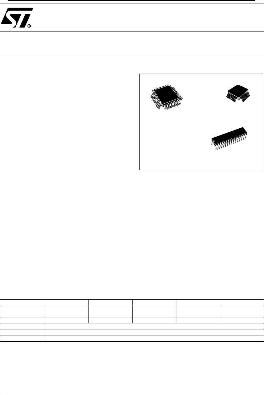
TQFP44
10 x 10
SDIP32
400 mil
TQFP32
7 x 7
Features ST72F324L(J/K)6 ST72F324L(J/K)4 ST72F324L(J/K)2 ST72324BL(J/K)4 ST72324BL(J/K)2
Program memory -
bytes
Flash 32K Flash 16K Flash 8K ROM 16K ROM 8K
RAM (stack) - bytes 1024 (256) 512 (256) 384 (256) 512 (256) 384 (256)
Voltage Range 2.85 to 3.6V
Temp. Range up to -40°C to +85°C
Packages TQFP44 10x10, SDIP32, TQFP32 7x7
1
DVD47 harman/kardon
87


