


2
AT24C01A/02/04/08A/16A
5092B–SEEPR–9/05
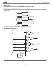
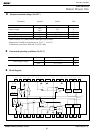
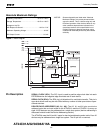
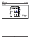
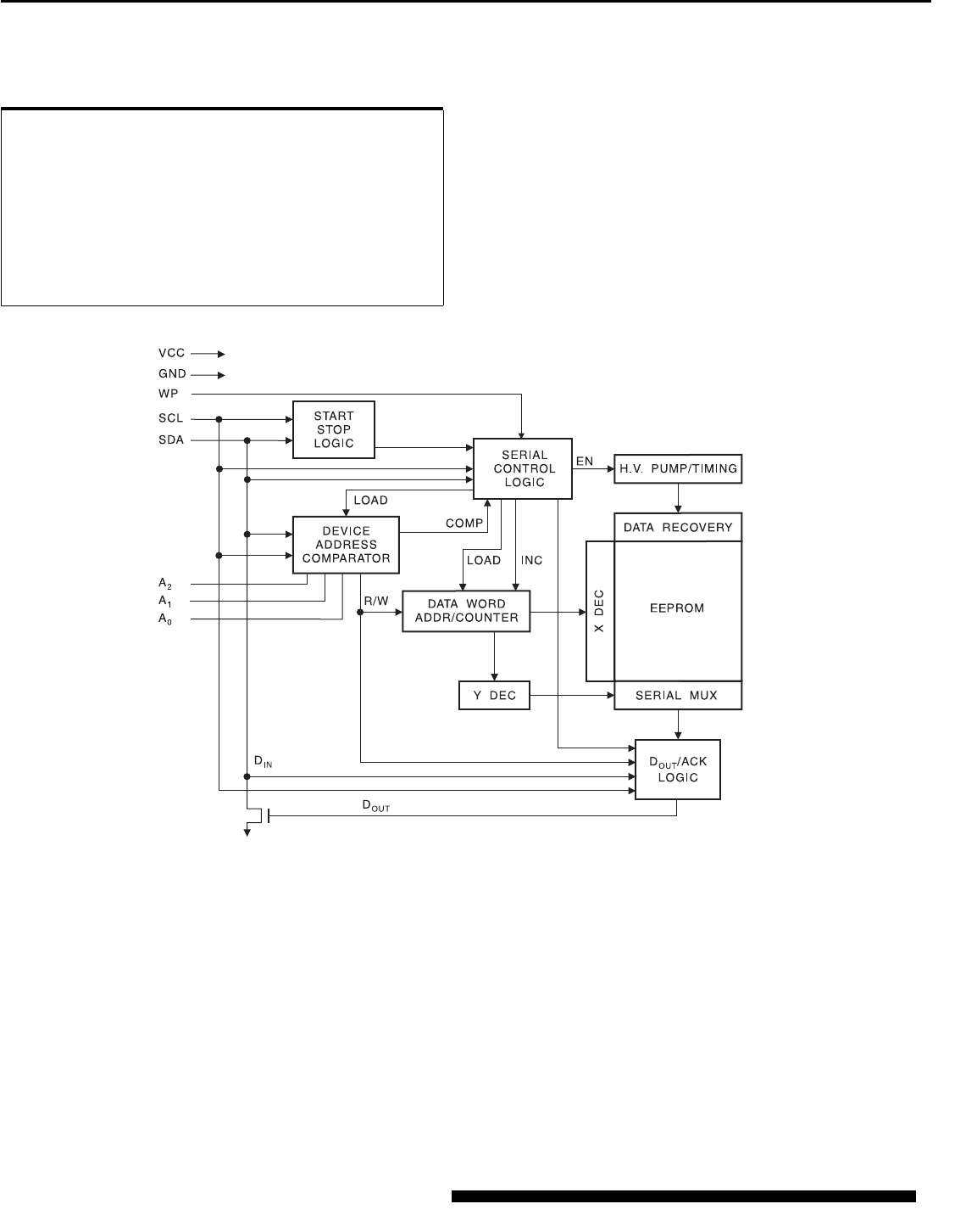
Figure 1. Block Diagram
Pin Description SERIAL CLOCK (SCL): The SCL input is used to positive edge clock data into each
EEPROM device and negative edge clock data out of each device.
SERIAL DATA (SDA): The SDA pin is bi-directional for serial data transfer. This pin is
open-drain driven and may be wire-ORed with any number of other open-drain or open-
collector devices.
DEVICE/PAGE ADDRESSES (A2, A1, A0): The A2, A1 and A0 pins are device
address inputs that are hard wired for the AT24C01A and the AT24C02. As many as
eight 1K/2K devices may be addressed on a single bus system (device addressing is
discussed in detail under the Device Addressing section).
The AT24C04 uses the A2 and A1 inputs for hard wire addressing and a total of four 4K
devices may be addressed on a single bus system. The A0 pin is a no connect.
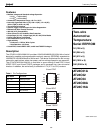
Absolute Maximum Ratings
Operating Temperature......................................−55°C to +125°C
*NOTICE: Stresses beyond those listed under “Absolute
Maximum Ratings” may cause permanent dam-
age to the device. This is a stress rating only and
functional operation of the device at these or any
other conditions beyond those indicated in the
operational sections of this specification is not
implied. Exposure to absolute maximum rating
conditions for extended periods may affect device
reliability.
Storage Temperature .........................................−65°C to +150°C
Voltage on Any Pin
with Respect to Ground........................................ −1.0V to +7.0V
Maximum Operating Voltage .......................................... 6.25V
DC Output Current........................................................ 5.0 mA
DVD47 harman/kardon
59