


ASUS P/I-P55T2P4 User’s Manual38
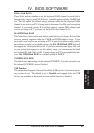
(Chipset Features)
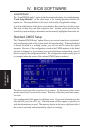
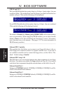
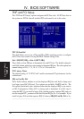
IV. BIOS SOFTWARE
IV. BIOS
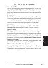
(Chipset Features)
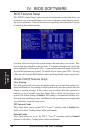
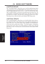
[DRAM and ECC]
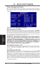
If all your DRAM modules have parity chips (e.g. 8 chips + 4 parity chips), they are
considered 36bits. This motherboard sums the memory per bank and therefore two
modules will give 72bits and the following will be displayed:
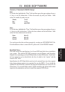
If your DRAM modules do not have parity chips (e.g. 8 chips), they are considered
32bits and the following will be displayed instead:
The default of Disabled for Memory parity SERR# (NMI) will not show memory
errors on your monitor. When using parity DRAM modules, you can select from the
default of Parity or ECC (Error Checking and Correcting) to correct 1 bit memory
errors that may occur in the memory. (See pages 12-13 for more information on
DRAM memory modules.)
......................................................................................................................................
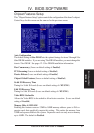
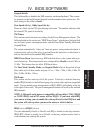
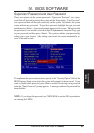
Onboard FDC Controller
When enabled, this field allows you to connect your floppy disk drives to the on-
board floppy drive connector instead of a separate controller card. If you want to
use a different controller card to connect the floppy drives, set this field to “Dis-
abled”. Default setting is Enabled.
Onboard FDC Swap A: B:
This field allows you to reverse the hardware drive letter assignments of your floppy
disk drives. Two options are available: No Swap (default) and Swap AB. If you want to
switch drive letter assignments through the onboard chipset, set this field to Swap AB.
Onboard Serial Port 1
Settings are 3F8H/IRQ4 (default), 2F8H/IRQ3, 3E8H/IRQ4, 2E8H/IRQ10, and Dis-
abled for the onboard serial connector.
Onboard Serial Port 2
Settings are 3F8H/IRQ4, 2F8H/IRQ3 (default), 3E8H/IRQ4, 2E8H/IRQ10, and Dis-
abled for the onboard serial connector.