


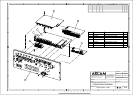

AVR400 Power Amplier Circuit Description
Apart from the power transformer, the power amplier electronics is fully contained on the large
double sided PTH PCB and heatsink located at the bottom of the AVR400. This is called the Main Board
on the schematic diagrams (pages 11 and 12). The Main Board also contains the mains input circuitry, in-
cluding the safety fuses and standby power transformer, so great care should be exercised when probing this
area of the board.
Note that some small surface mount components are soldered to the underside of this PCB.
The 7 power ampliers are identical in terms of circuitry, although necessary compromises in the physi-
cal layout may give rise to slight dierences in measured noise, crosstalk and distortion performance.
The two channels at the extreme ends of the heatsink have less radiating area available to them and will
run hotter under load – this is not normally an issue as these are assigned to the SBL and SBR channels.
Looking from the rear of the AVR, facing the at face of the heatsink, the channel order is SBR, SR, FR,
C, FL, SL and SBL, the same order as the loudspeaker terminals. The SBL and SBR channels can also be
assigned to zone 2 or as duplicates of the FL and FR channels for when passively biamping the main
stereo loudspeakers. In this latter condition we recommend assigning the SBL and SBR outputs to the
tweeters of the FL and FR speakers, in order to minimize the power ampliers’ heat dissipation.
Note that the 8 pre-amplier outputs are also on this PCB – apart from SUB their phono sockets are
eectively in parallel with the power amplier inputs, which are fed from the Input Board via a ribbon
cable and CON103. This connector also carries 5 power supply and power amplier control signals to
and from the system microprocessor (μP) IC151 situated on the Input Board above the Main Board.
The ampliers’ power supply is provided from a centre-tapped secondary winding on the toroidal
power transformer, via the connector BN508, to the bridge rectier D5830. This is mounted on a
small PCB near the top of the heatsink. The rectied AC is then sent to the main PCB via connectors
BN581/582. To avoid induced hum and distortion it is important to keep these cables twisted tightly
together and well away from the actual power amplier circuitry. The main 15,000μF 80V reservoir
capacitors, C835 and C836, are positioned on the main PCB well away from the power amplier input
traces and close to the system star ground. The smoothed DC is fed to the power ampliers’ Vcc and
Vee lines near the centre of the heatsink via a twisted-pair cable, again to minimize induction into the
power ampliers. Vcc and Vee are typically +/- 52V at 234VAC with no signal. Q5845 sends a fraction of
Vcc to the muting control on the Input Board.
The FL (front left) channel will now be described in detail.
The input stage is a long tailed pair Q5101 and Q5102, with local degeneration provided by R5105 and
R5107. The tail is fed from the negative rail via an approx 3mA ring-of-two constant current source,
Q5109 and Q5110. R5101 and C5101 at the input provide high frequency rollo and help keep residual
DAC ultrasonic noise above 100kHz out of the power amplier. DC blocking is provided by C5102 at
the input and C5107 in the feedback loop so that the whole power amplier has unity gain at DC. The
midband AC gain is 22000/680 = 32.35 after allowing for the attenuation provided by R5101 and R5102.
Thus 875mV at the input produces 100W into 8 ohms at the output.
The long tailed pair’s collectors are loaded by a current mirror, Q5103 and Q5104. The resistors R5103/4
and R5105/6 are 1% tolerance to minimize even order distortion. The collector of Q5101 also feeds the
Darlington class A voltage amplier stage (VAS) made up of Q5115 and Q5116. Q5113 is loaded by the
output stage and the 8mA constant current source made up by Q5125 and Q5126. The amplier’s main
frequency compensation network (for stability) comprises C5115 plus the combination of C5116 and
R 5115. This adds gain inside the loop (two pole compensation) at high audio frequencies so that the