


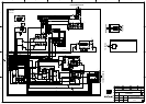
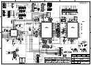
Q914 and Q915 (on the underside of the PCB) send BYPASS_ON and BYPASS_OFF logic signals from
IC906 to the array of 4 x 20-bit non-inverting line driver/bμFfers with tri-statable outputs, IC911/912 and
IC915/916. These are arranged as a 40 way 2-in, 1-out fast switch to bypass IC906 when required (e.g.
if 3D video is present). The video is in 12-bit RGB format and 4 more bμFfers are required for the video
clock, H and V syncs and the DE (data enable) line, thus using up all of the available 40 ways. See sheet 9
of the schematic diagram. Power is provided via local L-C decoupling from +3.3VH2.
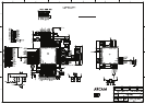
The HDMI output is handled by IC918, an Analog Devices ADV7511 in a 100 pin LQFP package. It is a
225MHz output part that can handle 12-bit 1080p video (up to 165MHz clock speed) and embedded HD
audio. It is compatible with certain parts of the HDMI 1.4 specication, supporting 3D video and an ARC
(audio return channel).
As with the other Analog Devices parts IC918 uses two power rails, namely +1.8VH2 and +3.3VH2. The
necessary decoupling capacitors are mounted on the underside of the PCB.
In the AVR400’s implementation the HDMI audio output is limited to stereo rather then 8 channels – via
I2S0 (pin 12), plus MCLK (pin 11), SCLK (pin16) and LRCLK (pin 17). SPDIF from the AVR400 is input to pin
10.
The ARC signal, if received from a downstream sink such as a TV, is output from pin 46 of IC918 and sent
via back to the input board. Note that IC921 is not tted.
The HDMI output is via JK97, a type A HDMI socket. As the AVR400’s output is partly HDMI 1.4 compliant,
pin 14 now becomes the HEAC+ and pin 19 HEAC- as well as HPD (Hot Plug Detect). However, because
the Ethernet part of the HDMI1.4 specication is not supported by the AVR400, the ARC is congured
by the sink to be carried in single (i.e. non-dierential) mode using HEAC+ as the signal line. HEAC+ and
HEAC- are then AC coupled to pins 52 and 51 of IC918 via the 1μF series capacitors C439 and C428. R771,
R777, R785, R795 and R799 bias the inputs and load the cable correctly.(Note – HEAC is short for HDMI
Ethernet and Audio (return) Channel).
Q916 is a twin n-channel MOSFET which only turns on when +5VH1 is present. This isolates the DDC
clock and data lines when the AVR400 is turned o.
IC917 is a low dropout voltage regulator feeding +5V power to pin 18 of JK97 from the +8VA supply,
when enabled by the SW_P+5V line.
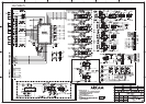
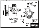
Analogue video output of digitized and processed 10-bit video from IC906 is available from the AVR400
via the video encoder IC919 – an Analogue Devices ADV7342B. Composite, s-video and component
video are supported, although only component analogue video is output by the AVR400.
IC919 is in a 64 pin LQFP powered from the +18VA and +3.3VA lines. Once again most decoupling com-
ponents are on the underside of the PCB.
The 6 x 11-bit video DACs inside IC919 are each loaded with 300R to ground before being AC coupled to
IC913. This is a JRC NJM2566 6-channel video amplier for SD and HD signals, powered from the +5VA
line. The FS_SEL signal on pin 17 sets the bandwidth on component video to 13.5MHz or 30MHz, to suit
progressive SD or HD signals respectively. The composite and s-video bandwidths are xed at 6.75MHz.
The outputs go to the analogue video daughter board via the 30 way socket BN301.
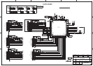
Note that the composite and s-video outputs are not actually used in the AVR400 so are not wired
beyond CN301 on the daughter board. The Y, Cr, Cb component video outputs are terminated with 75
ohm series resistors on the Analogue Video daughter board described next.