


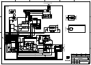
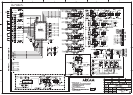
The HDMI input SOC, IC901, is a 144 pin LQFP Analog Devices ADV3014B. This is a 4 into 1 HDMI 1.4a
multiplexer and is connected to inputs 4 and 5 (VCR and PVR) on the rear panel (JK95 and JK96). The
other two inputs on IC901 are not used. The core power supply is +1.8V and the receiver terminator
supply voltage is +3.3V. Note that most power supply decoupling components are on the underside of
the PCB. +5V detect and hot plug assert control is carried out by the complementary pairs of switching
transistors Q904/907 and Q910/909. The video system clock is provided by a 28.63636MHz crystal X901
connected across pins 101 and 102.
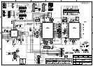
Pin 63 is set low by R602 meaning IC 901 is controlled by I2C at 3.3V via pins 78 (HDMI_SDA) and 79
(HDMI_SCL) from IC902. The HDMI output from IC901 is sent to input A of IC902.
IC902 is an Analog Devices ADV7844, packaged in a 425 pin BGA. It has a 4-input HDMI 1.3 receiver and
one video input supporting standard analogue video formats, from 525/625i up to 1080p, with 12-bit
ADCs. Its primary function is to prepare these signals for the main video processor IC906. Its second
function is to extract digital audio from the HDMI signals, including the reconstruction of a good quality
master clock, and to output all this in I2S or SPDIF format to the DSPs on the Input Board.
JK92 (AV), JK93 (SAT) and JK 94 (BD) connect to 3 of IC902’s HDMI input ports. Hot plug detect on
these 3 inputs is carried out by the complementary pairs of switching transistors Q905/906, Q908/901
and Q902/903. The 4
th
input receives the output of the HDMI switch IC 901. The core power supply is
+1.8VH2 and the receiver terminator supply voltage is +3.3VH2, with heavy local L-C decoupling. Note
that most of these power supply decoupling components are on the underside of the PCB. The video
system clock is provided by a 28.63636MHz crystal X902.
IC902 has a 256Mb SDRAM IC904 connected via 9 x 4-way 33 ohm resistor packs. This is used as a line/
frame store for digitizing the analogue video signals (CVBS, S-Video and Y, Cr, Cb) received from the
external video inputs and also separate i-Pod derived analogue video signals. It runs from the +2.5VH2
supply with further local decoupling components mounted on both sides of the PCB.
The 12-bit RGB video outputs are sent via 10 x 33ohm resistor packs to the tri-state bμFfers IC911 and
IC912. A 10-bit subset of these is also sent to the video processor IC906. Note that the critical video clock
is expanded to drive two output lines HD_VCLK1 (for IC906) and HD_VCLK2 (for IC911) via IC905 and 3 x
33ohm resistors.
The extracted digital audio outputs are sent as I2S and SPDIF signals to the audio DSPs on the input
board via 2 x 33 ohm resistor packs and the switch IC903. IC903 is enabled via Q913.
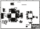
The video processor IC906 is an ST (formerly Genesis) “Torino” type FLI30336AC in a large 416 pin
BGA package. It is used to de-interlace and scale all the AVR400’s video inputs to the required output
resolution(s) up to 1080p and also to generate the system OSD (on screen display). Note that IC906’s
analogue video inputs are not used in this application and are either grounded via an array of resistors
and coupling capacitors close to one long edge of the heatsink or left open (R879-882 are no ts).
IC906 dissipates considerable power (about 4 watts) and is thus equipped with a heatsink soldered
to the PCB via two pins. Its core voltage is +1.8VH1, with +2.5V_DDR being used for its RAM bus and
+3.3VH1 for I/O and 19.66MHz crystal clock X903, all followed by copious local L-C decoupling. Note that
the decoupling capacitors and series inductors required are mounted on the underside of the PCB.
IC906 supports two 256Mbit DDR-1 500MHz 2.5V SDRAMs (IC908 and IC909) via a mix of 33R and 0R
series resistors in the data busses. On the other side of IC906 is its 32Mbit 3.3V ash memory IC907 (Ma-
cronix MX29LV320). IC931 is an Atmel AT24C64C 64K EEPROM with +3.3VH1 power.