


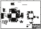

the necessary level shifting. IC73 includes internal charge pumps to convert CMOS logic level inputs
to +/-5V RS232 level outputs and +/-25V tolerant RS232 inputs to CMOS logic level outputs. Maximum
rated speed is 300kb/sec.
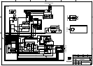
JK73 is a dual mono 3.5mm jack socket providing two +12V trigger outputs Z_1 and Z_2. The series pass
transistors Q712/715 are pnp T0-92 types with emitters referred to the +12V rail via the paralleled 4.7R
resistors R714/715 and R711/712. In conjunction with the pairs of diodes D711/712 and D714/715 this
provides current limiting at approximately 200mA if the trigger outputs are inadvertently shorted to
ground.
JK72 is a dual 3.5mm mono jack socket providing inputs for two modulated infra-red remote control
signals. These are connected to the opto-isolators IC72 and IC71. Note the use of the standby power
supply ST+5V for the subsequent logic.
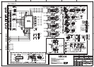
AVR400 HDMI Input/Output Board
The HDMI Board is described on pages 6 – 10 of the schematics diagrams. Note that it has components
tted to both sides of the PCB. HDMI stands for High Denition Multimedia Interface. The AVR400’s
system supports certain parts of the HDMI 1.4a specication (3D video compatibility and Audio Return
Channel)
The HDMI Board has 5 type A HDMI input sockets and one type A HDMI output socket, which are ush
with the back panel. It gets its power via the hard wired connector and ribbon cable CN61 and com-
municates with the Input Board via two ex foil cables attached to connectors CN104 (17 ways) and
CN105 (19 ways). It is tted with a 30 way socket BN301 which attaches to a daughter board handling all
analogue video I/O signals (the Analogue Video Board).
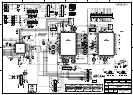
The HDMI Board contains 10 separately regulated local power supplies, mostly derived from the
unregulated but hum ltered +15V supply on the Power Supply Board. This is input on pins 3 and 4 of
the hard wired connector CN61 for +15V and pins 5, 6 and 7 for the ground returns. Pins 1 and 2 are not
used. See page 10 of the schematic diagram for all but the last of these supplies, as described below.
IC923, IC927 and IC930 are all Sanken SI-8005Q 3.5 Amps step-down switching regulators operating at
500kHz +/-10% and drawing power from the +15V line. They are used to generate +3.3VDD, +1.8VDD
and +1.8VH1 (video processor supply) respectively. The potential dividers in their outputs (R839+R844/
R847, R838+852/R851 and R841+843/840) are used to set the required voltages.
All other local power supplies use linear SM 3-terminal regulators.
IC922 and IC929 provide +2.5VH1 and +2.5VH2 for the two DDR memory chips supporting the video
processor. The source supply is +3.3VDD.
IC925 is a KIA7809 generating +8VA from the system’s +15VA line (NOT the unregulated +15V used
elsewhere on the board). This is further dropped to +5VA by IC924, a KIA1117S50. Inductor L860 provides
decoupling for the +5VH1 line. The video processor digital power supply lines +3.3VH1, +3.3VH2 and
+1.8VH2 are sourced from the +3.3VDD and +1.8VDD lines via L-C decoupling.
The video ADC’s analogue supplies, +3.3VA and +1.8VA, are generated from the +5VA line via IC926
(NJM2845DL133) and IC928 (NJM2845L118) respectively.
The 10
th
regulator, IC917, an NJU7754 found on sheet 9 of the schematic, is used to provide +5V to the
HDMI output socket. It is enabled via SW_P+5V and derives its input from the +8VA supply described
abov