


The surround and sub channels (IC205/206/208/209) are
very similar to the left channel described above except for
the op-amp ground references being tied directly to
0V_SIG. External multichannel inputs (FROM EXT
MAIN L, FROM EXT SURR L, etc) have 100pF NP0
capacitors to ground as an EMC preventative measure.
Volume control and headphones
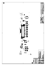
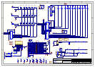
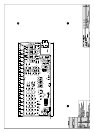
Refer to circuit diagram L921 sheet 5,6
Volume control is performed by a Burr-Brown PGA2310
volume control chip. This chip is pin and software
compatible with the Crystal Semiconductor CS3310
volume control chip. The only difference is that the
internal op-amps run off ±15 volts rather than ±5 volts.
The gain is under micro control with steps of 0.5dB. All
volume controls share data, clock and mute control lines
but have individual chip select lines. The volume of each
channel can be controlled individually. “Zero-crossing”
detect is permanently enabled on each volume chip to give
click-free volume changes. If, however, clicking can be
heard when changing volume, especially at higher levels,
it is likely that there is a dc offset into the volume control
chip. This points to an error in the previous stage which
should have removed all dc. The DCA XMUTE line is a
power-on mute with a time constant set by R703 and C701
(sheet7). The output op-amps (IC 502, 505 etc) are
configured to block dc and are inverting amplifiers to
restore the polarity of the signal as the volume control
chips are non-inverting.
Since all outputs are identical only the main left output
around IC502A will be described. IC501 is a self
contained volume control with non-inverting op-amp.
C501 prevents oscillation of IC502A. C507 blocks dc to
subsequent stages of the circuit but is in the feedback path.
This provides some compensation for capacitor non-
linearities. R527 provides a local dc path to prevent the
op-amp latching into rail. R502 provides output
protection, limiting current in the event of the output being
shorted. R503 provides a weak 0V reference to prevent
the output floating. IC503 is a DG413 analogue switch
which acts as a mute under micro control via
demultiplexer IC708. The five DG413s play a vital role in
preventing thumps at turn on/off.
At power on, the MAIN OUTS ENABLE and ZONE 2
OUTS ENABLE lines are forced low in hardware, pulling
the output connectors to ground. The hardware control of
these lines is determined by an RC time constant (see
‘control lines from micro’ below for details). This
allows sufficient time for the micro to boot up and take
control of these lines.
At power off, the micro detects power loss and forces the
outputs into the mute (grounded) state. This prevents any
pops. However, if the DG413s were run directly off the
+/- 15V rails, the outputs were found to drift to a dc level
that tripped power amplifiers into dc protect. This was due
to the way the power rails collapsed. (The -15V rail
actually went slightly positive for a time causing the dc
output drift.) D506 and D507 isolate the output mutes
from the main +/-15V supply. C543 keeps the supplies to
the output mutes up until long after the main +/-15V rails
have completely collapsed. R537 and R538 are actually
capacitors to decouple both local supplies to ground.
D503 protects the output stage by shunting over-voltage
spikes to the power rails. (It should be noted that the
diodes are not power devices, therefore they are likely to
fail if a high energy pulse is fired up the outputs of the
unit.) C502 shunts any high frequency signals at the
output to ground to help EMC.
The source for the headphone can be from the MAIN
output (IC502) or ZONE2 (IC505). Selection is by
74HCT4053 multiplexers IC507 and IC508 under micro
control via control line demultiplexer IC708. IC509 is an
LM4880 headphone driver IC which runs off the +5V
(analogue) rail. Its supply is drawn through a 2.2ohm
resistor to try to provide some crosstalk isolation to the
input multiplexers +5V power rail.
Zone2 and record loop outputs
Refer to circuit diagram L921 sheet 4
The input switches on schematic page 1 mix onto a virtual
earth bus (ZONE2, TAPE OUT or VCR OUT). The
associated op-amps are found here. Zone2 (IC401) has the
same type of dc blocking circuit as described before for
sheet 2 of the schematics. Note however that the feed
forward resistor is 100kΩ. To maintain unity gain, the
feedback resistors R402 and R404 have been chosen such
that their value in parallel with 1MΩ equates to 100kΩ.
TAPE and VCR record outputs (IC402 and IC403) have
100kΩ as the feedback resistor in series with a 47Ω output
protection resistor. The outputs are capacitively coupled
without compensation with a weak 100kΩ pull-down to
0V_SIG to prevent the outputs floating off.
Control lines from the micro
Refer to circuit diagram L921 sheet 7
Control lines for individual switches etc are derived from
16-bit words sent as serial data to three sets of serial to
parallel latches (port expanders). In this way, many local
control lines can be provided whilst only using a few
micro I/O ports. The same data and clock lines also drive
the PGA2310 volume control chip. IC702 decodes chip
selects for the volume control and latch devices. On
power up, the contents of the latches is cleared using a
buffered R-C circuit (R703, C701, IC701E/F). This also
mutes the volume control chips. In practice however, this
latch clear and volume mute line is of limited use as the
+5V analogue supply collapses slowly. If the unit is
switched off and back on within a period of 5 seconds,
C701 will not have discharged via D701 sufficiently for
the input of Schmitt trigger IC701E to interpret a LOW
condition. The default power-on state for the volume
control chips mute in any case.
IC708 is a special case as it provides the control of the
MAIN and ZONE 2 OUTS ENABLE. These must
be low
at power up to prevent turn-on thumps, due to the
initialisation time period of the micro this must be done in
hardware. C710 and R729 generate a line that is HIGH at
switch-on, which sets the output of the latch to tristate
(high impedance). R535 and R536 pull these lines low so
that the output mute ICs switch the outputs to ground,
theoretically keeping the outputs silent during power-up.
In practice a small tick may be heard because the logic
devices don’t begin to operate properly until they have a
few volts across them. C710 charges via R729 over a
period of approximately one second. The falling OE line
to IC708 enables the latch outputs, which have by now
been written to by the uC.
Power supply
Refer to circuit diagram L921 sheet 8
The board is powered from the +/-18V and +21V supplies
which are regulated using standard LM317T and