


Overcurrent Protection
A number of mechanisms protect the PSU in the event of a
short circuit or very high load being placed on one of the
outputs.
The PSU has a power limit of around 45W. If an attempt is
made to draw more power than this then the PSU will
power limit. This will show up as a reduction in the output
voltages. This will in turn force the feedback loop to
attempt to demand more power throughput to correct the
low output voltages. The feedback signal will then trigger
the feedback loop failure mechanism which will then force
the PSU into latched shutdown if this persists for more
than around 1second.
Mains Present Signal
The PSU provides a signal MAINSOK* (active low when
mains supply is OK). This signal is provided as an open
collector signal from SK8-2. The signal will go high (via a
pull-up resistor external to the PSU) when the mains
supply is removed and will then provide > around 20mS
warning of the imminent collapse of the output rails.
The actual time between the rising edge of MAINSOK*
and the output voltage rails falling out of spec is dependent
on mains input voltage and output load current. The output
voltages will hold up longer when the load current is low
and the mains input is high. The 20mS hold up spec is
based on low mains voltage and full load.
Inrush current protection
The PSU has an NTC in series with the input reservoir
capacitor. When the supply is first powered up the NTC is
cold and exhibits a resistance of around 25Ohms which
limits the current into the capacitor and prevents damage to
the capacitor, fuses and mains switch. After several
seconds the NTC temperature rises to around 90C and the
resistance falls to a low value allowing normal operation.
PSU Over-temperature Protection
The PSU transformer is fitted with a one shot thermal fuse.
This opens at 120C and removes the supply to the primary
side controller. The thermal trip is taped to the outside of
the transformer so that it could in principal be changed.
The materials from which the transformer is constructed
are rated for operation at 130C and in normal operation the
TX surface temperature is < 90C.
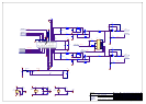
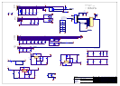
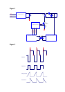
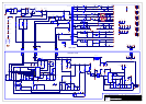
Figure 1
This diagram shows a very simplified PSU block diagram.
Only one output is shown and the active clamp is omitted.
The basis operation is as follows.
At the beginning of the switching cycle the gate drive
signal to M2 goes high. M2 is turned ON and the voltage
across C35 is applied across the primary of L1. During this
stage the voltage on the anode of Dout is negative the
diode is reverse biased and no current flows in the
secondary winding. The voltage applied across the primary
causes the current in L1 primary to ramp up from zero.
When the control circuit turns off M2 by taking gate drive
low then the bottom of the inductor flies back above the
input voltage . This flyback action causes the output diode
Dout to conduct and current is transferred to the output
capacitor Cout.
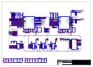
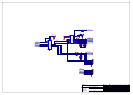
Figure 2
These waveforms are for a non resonant ordinary
discontinuous flyback supply to illustrate the operation of
the circuit. The drain waveform starts at the voltage on the
input capacitor C35 and falls to near zero when the mosfet
is switched on. When the mosfet is switched off the drain
voltage flies above the input voltage and produces the
ringing waveform as shown. The current then ramps down
into Cout. When the current has fallen to zero there is
again some ringing. The frequency of the ringing is
dependent on circuit parasitics.
The primary current can be viewed by looking at the
voltage across R30. The output diode current can be
measured by using a current probe around Dout or inferred
by looking at the voltage waveform across Cout. The
falling ramp should produce a small voltage ramp across
the ESR of Cout.
By considering the simplified circuit it can be seen that all
of the output rails are developed in the same way. The
output diodes provide current to the large reservoir
capacitors on each rail.