


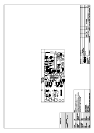
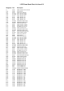
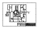

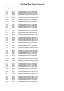
SK1000
Pin1 P18V
Pin2 AGND
Pin3 N18V
Pin4 P21V
Pin5 AGN
Pin6 N21V
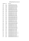
SK1001
Pin1 P12V
Pin2 DGND
Pin3 N12V
Pin4 DGND
Pin5 P5V
Pin6 DGND
Pin7 P3V3
Pin8 DGND
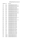
SK1002
Pin1 PSU SYNC
Pin2 PSU GOOD
Pin3 PSU KILL
Pin4 DGND
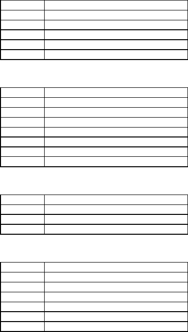
SK1003
Pin1 P36VF1
Pin2 0VF1
Pin3 P36VSET
Pin4 P5VF2
Pin5 OVF2
Pin6 P5VF2SET
Pin7 N/C
ADC
Refer to circuit diagram L896 Sheet 2
The signals to the ADC are converted to balanced by the three
opamps that also correct the level to the input of the ADC so
that 2VRMS on the input of the first opamp provides a full-scale
input to the ADC. 2.45V p-p (Note: not RMS)
A bias is added to the incoming signal so that it can be input to
the ADC analogue section which operates on a single 5V rail.
The bias is generated by the potential divider R216 and R217
this is 1.75V it is amplified by 1.43 by the opamp to give
approximately 2.5V at the output of the opamps IC202 and
IC203.
The diodes D200, D201, D202, D203 prevent over voltage
signals from being presented to the input of the ADC, they do
not protect the ADC if one of the opamp fails, as the diode will
blow as well. The ADC itself is set to operate as a master for the
I2S interface and to have its internal high pass filter enabled.
Data is output from the ADC on pin 15, it also generates a bit
clock at 64xFS on pin 14 and a word clock at Fs on pin 13. The
master clock on pin 17 is an input and should be at 256xFs.
DAC
Refer to circuit diagram L896 Sheets 3,4,5,6
The DAC sheets are all essentially the same and so are only
described once below. The Sub DAC output has some minor
differences that are described in the text.
The DAC is a 24bit 192KHz part it consists of a serial interface
port, digital interpolation filter, multi bit sigma delta modulator
and stereo DAC. The DAC is in hardware configuration mode
(the control of emphasis and serial interface mode is set by
pulling pins high and low on the DAC). The serial interface is
set to I2S. The pins DM0 and DM1 control the de-emphasis
filters and are controlled via a serial to parallel latch (IC905)
connected to the micro.
DAC reset is used to initialise the part and is under the control
of the microprocessor via a latch (IC905), it is an active low
signal. DAC MUTE on the same latch is an active low signal
and forces a soft mute of the output of the DAC.
The serial audio data interface consists of the DAC I2S LRCLK,
DAC I2S BCLK and DAC I2S DATA.
DAC I2S LRCLK is the left right clock for the audio frames it
should be a square wave at the sampling frequency. The signal
is low during the left frame and high during the right frame.
DAC I2S BCLK is the bit clock for the data and data is clocked
into the DAC on the rising edge of this clock. The bit clock
operates at 64 times the left right clock.
DAC I2S DATA is the actual audio data it is should be
presented in I2S format that is one bit offset MSB first data of
up to 24bits. Each data frame consists of 32bits one offset bit 24
data bits and 7 empty zero bits. (If the actual data is less than 24
bits (i.e. from CD) the unused bits may also be empty zero.)
The output of the DAC is differential on the pins 16,17 for left
and 12,13 for right. This signal passes into a second order
multiple feedback type balanced to single ended filter. The filter
is a second order Bessel function with a three dB point of
approximately 75KHz. This filter has been reworked on the
Bass output to have a three dB point of approximately 300Hz to
reduce the HF noise introduced by the bass management section.
The filter is unity gain however the balanced to single ended
conversion introduces a gain of two. The output of the balanced
to single ended converter should be 2Vrms for a full scale input.
Following the filter is a buffer stage. The buffer stage performs
two functions, it is a virtual earth mixer used to mix bass
information into the other channels when a sub woofer is not
present. Switching the CMOS switch 74HCT4053 controls the
mix. The control of the CMOS switch is under microprocessor
control via a latch (IC904). The second function of the buffer is
to provide a ground sense to the Audio board. This allows the
two boards to be loosely connected via a high impedance
without introducing hum. The difference between the grounds
on the two PCBS is sensed by the positive input of the opamp
and added into the signal, this effectively removes any ground
variation between the two PCBS. The full-scale output of the
DAC should produce 2v RMS at the output of the buffer stage.
DAC performance specification
THD better than -95dB (0.0018%)
Noise level at output of buffer better than -100dB ref 2VRMS or
94dBV
Frequency response +/- 0.4dB 10Hz to 20KHz
The other components on the circuit are decoupling for the
DAC, OPAMP and CMOS multiplexer. VMIDR and VMIDL
are the output bias chains and should be at approximately half
the Analogue Voltage rail (2.5V). AVDDL and AVDDR are the
logic supply rails for the digital filter and the switched capacitor
filter.
DSP
Refer to circuit diagram L896 Sheet 7
This is the Digital signal Processor sheet. IC701 is the main
DSP it decodes the in coming data stream to provide the 5
channels of discrete audio from Dolby Digital, DTS or MPEG
encoded material or a matrix decode of stereo information to 4
or five channel. The decoded data is passed to the second DSP
IC702 that performs post processing on the signal, performing
the THX equalisation Tone controls and Bass management.